
Circuit Diagram
Index 1236
SWITCHING_CLICK_SUPPRESSOR
Published:2009/6/29 23:39:00 Author:May
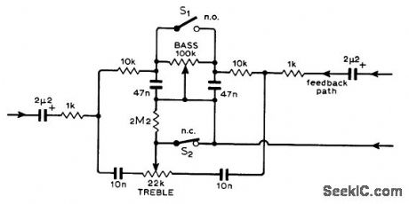
Correction network shown can be inserted in audio channel of mixing console without producing transients or level changes. Although Baxandall network is shown, switching technique is applicable to other filters. With S1 normally open and S2 normally closed, circuit operation is normal. If switch positions are simultaneously reversed, response remains flat regardless of positions of bass and treble pots, centerfrequency gain remains unchanged, and phase shift is unchanged. There is then no transient interruption of AF signals. Switching clicks cannot occur because there is no direct current in the network.-J. S. Wilson, Click-Free Switch-ing forAudio Filters, Wireless World, Jan. 1975, p12. (View)
View full Circuit Diagram | Comments | Reading(744)
High_speed_low_noise_instrumentation_amplifier
Published:2009/7/24 21:47:00 Author:Jessie

Figure 6-12 is similar to Fig. 6-1, except for the op-amp characteristics. For the LT1028, the input voltage-noise density is 1.1 nV√Hz maximum at 1 kHz, 0.85 nV√Hz typical at 1 kHz, 1.0 nV√Hz typical at 10 Hz, and 35 nVp-p typical at 0.1 Hz to 10 Hz. Minimum gain-bandwidth is 50 MHz, minimum slew rate is 10 V/μs, maximum offset voltage is 40 μV, and maximum offset drift is 0.8 μV/℃. Minimum voltage gain is 7 million. MAXIM NEW RELEASES DATA BOOK, 1993, P. 3-59. (View)
View full Circuit Diagram | Comments | Reading(920)
Wideband_fast_settling_op_amp_with_multplex_input
Published:2009/7/24 21:45:00 Author:Jessie
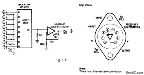
Figure 6-11 shows a BB3554/MX3554 used with a MAX310 to provide eight channels of video signal to a single cable. The op amp slews at 1000 V/μs and provides up to ±100 mA output with±10-V supplies. MAXIM NEW RELEASES DATA BOOK, 1993, P. 3-43. (View)
View full Circuit Diagram | Comments | Reading(708)
Ultra_fast_ECL_output_comparator
Published:2009/7/24 21:43:00 Author:Jessie
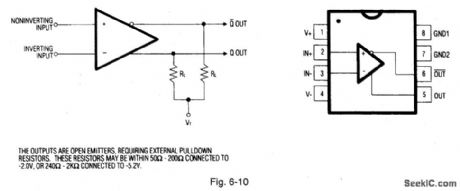
Figure 6-10 is similar to Fig. 6-9, but without the latch-enable function. Propagation delay is 1.3 ns. MAXIM NEW RELEASES DATA BOOK, 1993, P. 3-41. (View)
View full Circuit Diagram | Comments | Reading(730)
Ultra_fast_ECL_output_comparator_with_latch_enable
Published:2009/7/24 21:42:00 Author:Jessie
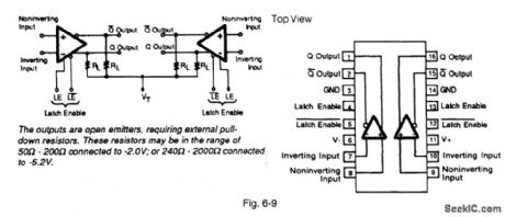


Figure 6-9 shows a MAX9687 connected as a fast (600 MHz) output comparator under latch control. The latch-enable inputs can be driven from a standard ECL gate. When LE is high and LE is low, the comparator function is normal. When LE is low and LE is high, the comparator outputs are locked in the logic states determined by the input conditions at the time of the latch transition. If the latch-enable function is not used, connect LE to ground and leave LE open. The propagation delay is 1.4 ns, the latch setup time is 0.5 ns, the latch-enable pulse width is 2.0 ns, and the power supplies are +5 V and -5.2 V. MAXIM NEW RELEASES DATA BOOK, 1993, P. 3-39. (View)
View full Circuit Diagram | Comments | Reading(1188)
LINEAR_1_4_VOLUME_EXPANDER
Published:2009/6/29 23:39:00 Author:May
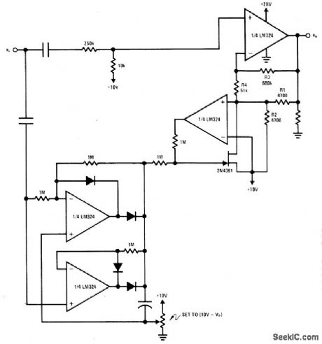
Gain varies automatically with strength of input signal, being lowest for weak signals. Resistors R3 and R4 modify linear control curve to give log curve desired foraudio systems. Overall gain of circuit is about 0 dB at midrange of expansion. Lower pair of LM324 quad opamp sections function as full-wave precision linear peak detector. For stereo, only upper part of circuit needs to be duplicated for second channel.- Linear Appli-cations, Vol. 2, National Semiconductor, Santa Clara, CA, 1976 AN-129 p 7. (View)
View full Circuit Diagram | Comments | Reading(816)
CLIPPER
Published:2009/6/29 23:38:00 Author:May
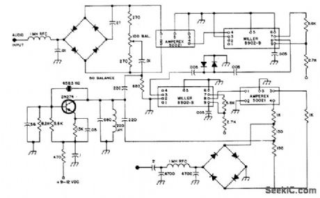
Provides speech clipping at BF level for SSB transmitters. Based on use of two Amperex 455-kHz IF crystal filters having 4-kHz rated bandwidth, in place of costly conventional sideband filters. Miller 8902-B IF amplifier module simplifies wiring. Diode balanced modulator at upper left can use individual 1N63 or 1N914 diodes, or FICA CA.3019 hex diode array that also provides diodes for RF clipper. Audio input can be taken from speech compressor of re celver, or separate audio amplifier can be added to boost AF level. Same diode types are used in product detector for final SSB signal, lower right, which is diode ring demodulator taking in jection voltage from carrier oscillator. Article tells how pin 8 on IF module (not connected in-temally) is bridged to solder line between link output of last IF transformer and AM detector diode, and gives other construction details.-J.J. Schultz, Inexpensive RF Speech Clipper, 73 Magazine, Sept. 1974, p 61-64 and 66. (View)
View full Circuit Diagram | Comments | Reading(1)
BAXENDALL_TONE_CONTROL_CIRCUIT
Published:2009/6/29 23:22:00 Author:May
View full Circuit Diagram | Comments | Reading(608)
PASSIVE_BASS_&_TREBLE_TONE_CONTROL
Published:2009/6/29 23:22:00 Author:May
View full Circuit Diagram | Comments | Reading(723)
ACTIVE_BASS_&_TREBLE_TONE_CONTROL_WITH_BUFFER
Published:2009/6/29 23:20:00 Author:May
View full Circuit Diagram | Comments | Reading(1244)
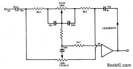
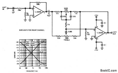
AMPLIFIER_WITH_BASS_BOOST
Published:2009/6/29 23:20:00 Author:May
View full Circuit Diagram | Comments | Reading(1135)
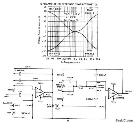
IC_PREAMPLIFIER_WITH_TONE_CONTROL
Published:2009/6/29 23:19:00 Author:May
View full Circuit Diagram | Comments | Reading(840)
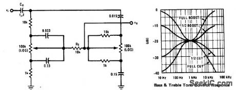
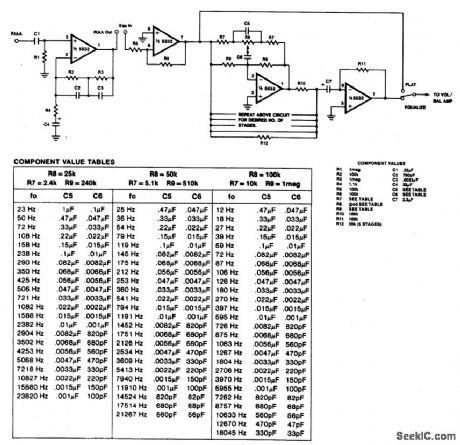
THREE_CHANNEL_TONE_CONTROL
Published:2009/6/29 23:18:00 Author:May
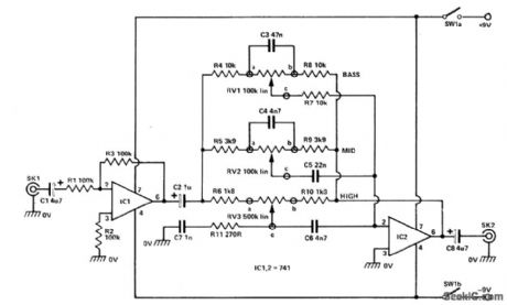
The input signal is fed via SKI to the first active stage built around IC1. Configured as a noninverting amplifier whose gain is set by the ratio of R3 and RI. In this case, the gain is set at unity. This initial stage is required to isolate the following stage from any loading effects. The output from IC1 is fed via three frequency shaping networks to IC2. The three networks built around RV1, RV2, and RV3 are also in-cluded in the feedback path of IC2, another inverting op amp stage. The components as-sociated with the three variable resistors are chosen to give the required frequency control. (View)
View full Circuit Diagram | Comments | Reading(824)
EQUALIZER
Published:2009/6/29 23:17:00 Author:May
View full Circuit Diagram | Comments | Reading(0)
STEREO_PHONOGRAPH_AMPLIFIER_WITH_BASS_TONE_CONTROL
Published:2009/6/29 23:16:00 Author:May
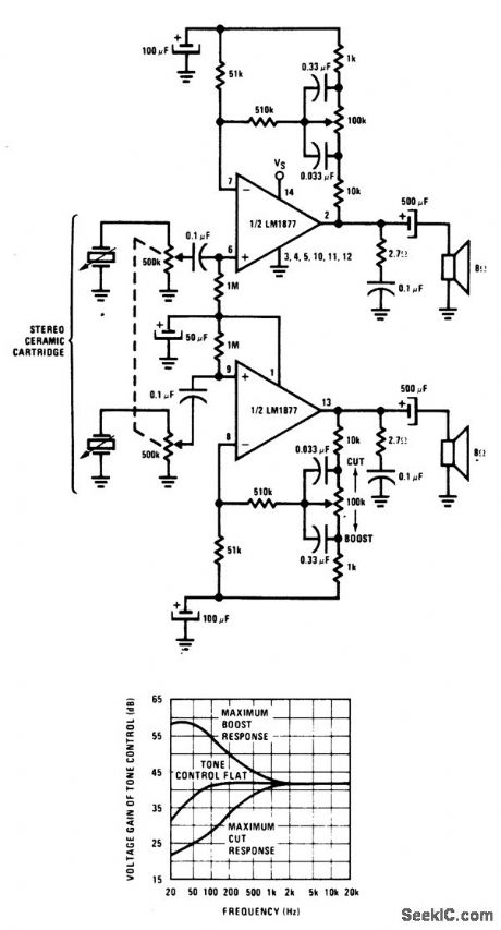
View full Circuit Diagram | Comments | Reading(815)
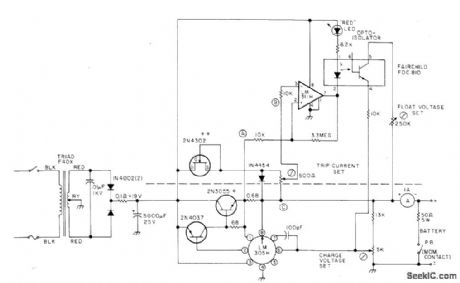
GELLED_ELECTROLYTE_BATTERIES
Published:2009/6/29 23:05:00 Author:May
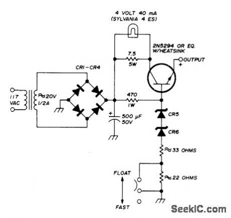
Constant-voltage charger for Globe-Union 12-V gelled-electrolyte storage batteries can provide either fast or float charging. Constant voltage is maintained by series power transistor and series-connected zeners. Output voltage is 13.8 V for float charging and 14.4 V for fast charging.-E. Noll, Storage-Battery QRP Power, Ham Radio, Oct. 1974, p 56-61. (View)
View full Circuit Diagram | Comments | Reading(2443)
NICAD_CHARGE_CONTROL
Published:2009/6/29 23:04:00 Author:May
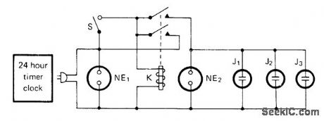
Prevents doublecharging if someone forgets to turn off 24-h time clock after recommended 16-h charge period. Nicad devices with built-in chargers are plugged into jacks J1-J3, and timer dial is advanced until clock switch is triggered. Neon lamp NE1 should now come on. Momentary pushbutton switch S is pushed to energize relay K and start charge, When timer goes off, K releases to end chatge.-M. Katz, Battery Charge Monitor, CQ, July 1976, p 27. (View)
View full Circuit Diagram | Comments | Reading(672)
ACTIVE_RC_FILTER_FOR_FREQUENCIES_UP_TO_150_kHz
Published:2009/6/29 23:03:00 Author:May
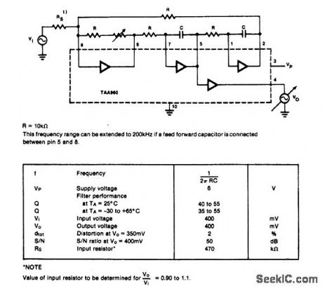
View full Circuit Diagram | Comments | Reading(651)
12_V_FOR_GELLED_ELECTROLYTE
Published:2009/6/29 23:02:00 Author:May
Designed to charge 12-V 3-Ah gelled-electrolyte battery such as Elpower EP1230A at maximum of 0.45 A until battery reaches 14 V, then at constant voltage until charge current drops to 0.04 A. Charger is then automatically switched to float status that maintains 2.2 V per cell or 13.2 V for battery. Circuit is constant-voltage regulator with current limiting as designed around National LM305H, with PNP/NPN transistor pair to increase current capability. Circuit above dashed line is added to standard regulator to meet special charging requirement. Article covers operation and use of circuit in detail.-H.Olson, Battery Chargers Exposed, 73 Magazine Nov.1976, p 98-100 and 102-104. (View)
View full Circuit Diagram | Comments | Reading(865)
TUNABLE_ACTIVE_FILTER
Published:2009/6/29 23:01:00 Author:May
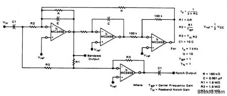
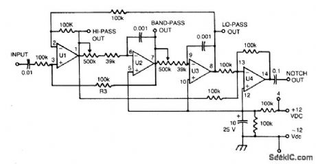
Circuit NotesThe high-pass and low-pass outputs cov-ering the range of 300 Hz to 3000 Hz have been summed in the fourth op amp to provide a notchoutput. The potentiometers must have a re-verse log taper. Fixed-frequency active filter center frequency is1 kHz, with a Q of 50. (View)
View full Circuit Diagram | Comments | Reading(951)
| Pages:1236/2234 At 2012211222122312241225122612271228122912301231123212331234123512361237123812391240Under 20 |
Circuit Categories
power supply circuit
Amplifier Circuit
Basic Circuit
LED and Light Circuit
Sensor Circuit
Signal Processing
Electrical Equipment Circuit
Control Circuit
Remote Control Circuit
A/D-D/A Converter Circuit
Audio Circuit
Measuring and Test Circuit
Communication Circuit
Computer-Related Circuit
555 Circuit
Automotive Circuit
Repairing Circuit