
Circuit Diagram
Index 1228
CLAMPING_WITH_OPAMPS
Published:2009/6/30 2:12:00 Author:May
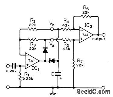
Circuit is used after stage of AC amplification to damp minimum level of signal voltage to 0 V for signals having amplitudes between 10mV and 10V.With 250-μF electrolytic for C, sinusoidal waveforms between 3 and 10,000 Hz are clamped with little distortion. Overall gain is unity,-C.B. Mussell, D.C.Level Clamp, Wireless World, Feb. 1975, p 93. (View)
View full Circuit Diagram | Comments | Reading(975)
AF_COMPRESSOR
Published:2009/6/30 2:12:00 Author:May
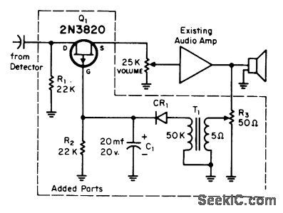
Developed for use in communication receiver where signals vary so greatly that even modern AVC systems cannot level all signals. Circuit is AVC that sets miaxmum audio level which will not be exceeded.Uses one FET as series attenuator controlled by DC voltage derived from audio output. R3 permits adjustment of compression leveL-C.E.Richmond, A Receiver Audio Compressor, CQ June1970,p 35 and 86. (View)
View full Circuit Diagram | Comments | Reading(1449)
CRO_HIGH_VOLTAGE_SUPPLY
Published:2009/6/30 2:11:00 Author:May
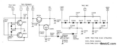
Controlled inverter operates from 12-V battery and feeds positive and negative triplers for producing ±600 V required for portable CRO, T601 high-voltage transformer has 22K,5.2K、and 600-ohm windings,all center-tapped,often marked Lionel when available in surplus shops,Q201,Q202、and Q204 are 2N697 or 2N2219,Q203 is 2N4302 or 2N5457.—G.E.Friton,Eyes for Your Shack,73 Magazine, Magazine,Nov./Dec,1975,p 74-76、78-88、and 90-94. (View)
View full Circuit Diagram | Comments | Reading(1761)
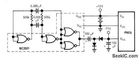
12_V_TO__11_V_WITH_TRANSISTORS
Published:2009/6/30 2:09:00 Author:May
Bipolar inverter and rectifier together provide -11 V from 12-V auto battery for operdting highthreshold MOS logic of portable or automotive equipment. Transistor and diode types are not critical. Multivibrator draws only 1.2 mA from battery on standby and supplies 12 mA from negative output terminal.—B. Fette, Inexpensive Inverters Generate VGG for Portable MOS Applications, EDN|EEE Magazine, Dec.15, 1971, p 51. (View)
View full Circuit Diagram | Comments | Reading(958)
28_V_HIGH_EFFICIEIVCY
Published:2009/6/30 2:09:00 Author:May
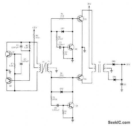
Uses driven-type converter in which signal source is simple two-transistor oscillator Q1-Q2. Turn-on delay technique eliminates overlap current otherwise flowing in 2N1016 push-pull power transistors Q5 and Q6 when one is still on in storage state while other is driven on. Efficiency can approach 90%. Q3 and Q4 prevent off transistor from conducting until opposite device has turned off. Values for T2, CR3, and CR4 in output circuit are chosen to give desired DC output voltage.—R. F. Downs, Minimize Overlap to Maximize Efficiency in Saturated Push-Pull Circuits, EDN|EEE Magazine, Feb. 1, 1972, p 48-50. (View)
View full Circuit Diagram | Comments | Reading(560)
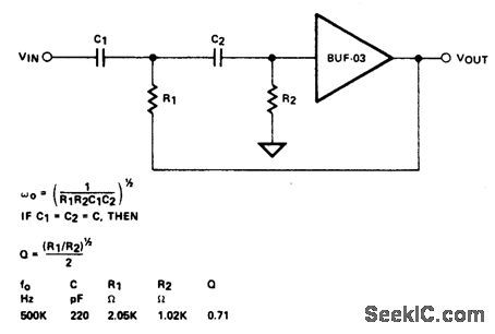
160_Hz_BANDPASS_FILTER_
Published:2009/6/30 2:07:00 Author:May
View full Circuit Diagram | Comments | Reading(672)
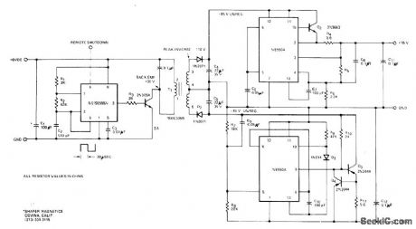
CRO_LOW_VOLTAGE_SUPPLY
Published:2009/6/30 2:07:00 Author:May
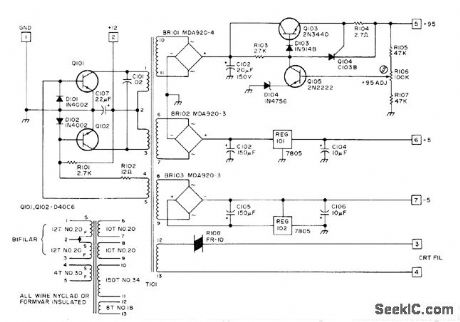
Developed for use as one of supplies for portable CR0, operating from battery using sealed rechargeable cells supplying 12 V at 2-5 Ah. High-efficiency inverter uses two GE D40C6 or RCA 2N5294 transistors (D101 and D102) as commutating switches for untapped feedback winding of power transformer. R102 then determines drive, while R101 produces required unbalanced starting bias. Thermistor R108 in series with CRT filament has cold resistance of 10 ohms to counteract very low cold resistance of CRT filament at start-up and prevent inverter malfunction. Article gives instructions for winding T101, along with high-voltage supply circuit and all other circuits of CRO covering DC to 10 MHz.—G. E. Friton, Eyes for Your Shack, 73 Magazine, Nov./Dee. 1975, p 74-76, 78-88 and 90-94. (View)
View full Circuit Diagram | Comments | Reading(1094)
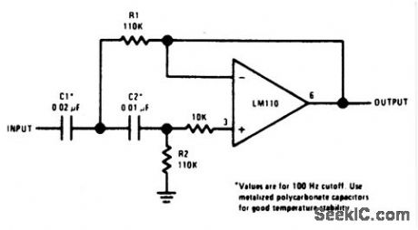
SECOND_ORDER___HIGH_PASS_ACTIVE_FILTER___
Published:2009/6/30 2:07:00 Author:May
View full Circuit Diagram | Comments | Reading(830)
TWO_OUADRANT_EXPONENTIAL_CONTROL
Published:2009/6/30 2:06:00 Author:May
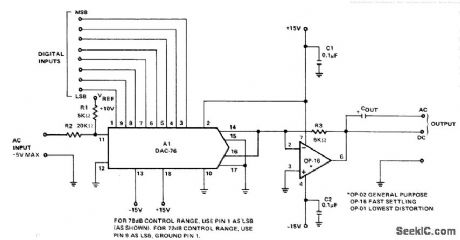
Decibel-weighted control characteristic of Pre-cision Monolithics DAC-76 DIA converter matches natural Ioudness sensitMty of human ear, to provide much greater useful dynamic range for controlling audio Ievel. Control range can be either 72 or 78 dB, depending on pin connections used. 8-bit word control input can be interfaced with standard TTL-compatible microprocessor outputs. To avoid annoying output transients during large or rapid gain changes, use clickless attenuatoriamplifier (also given in application note).-W. Jung and VV.Ritmanich, Audio Applications for the DAC-76 Companding D/A Converter, Precision Mono-Iithics, Santa Clara, CA, 1977, AN-28 p 2. (View)
View full Circuit Diagram | Comments | Reading(965)
LOW_CURRENT_INTRUDER_ALARM
Published:2009/6/30 2:05:00 Author:May
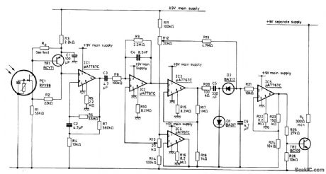
Use of programmable μA776 opamps reduces standby current of infrared alarm to 300 μA, permitting operation from small rechargeable cells. Detector is Mullard RPY86 that responds only to wavelengths above 6 μm, making it immune to sunlight and backgrounds intermittently illuminated by sun. Low-cost mirror is used instead of lens to concentrate infrared radiation on detector. Rd is chosen to make input to first opamp between 2 and 6 V. Circuit energizes alarm relay RL only when incident radiation is changed by movement of intruder in monhored space.- Ceramic Pyroelectric Infrared Detectors, Mullard, London, 1978, Technical Note 79, TP1664, p 8. (View)
View full Circuit Diagram | Comments | Reading(861)
SQUELCHABLE_AMPLIFIER
Published:2009/6/30 2:05:00 Author:May
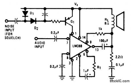
Circuit designed for portable FM scanners and two-way walkietalkie radios can be tumed off by noise or by control signal to minimize battery drain. When squelched, LM388 opamp-transistor-diode anay draws only 0.8 mA from 7.5-V supply.Diodes rectify noise from Iimiter or discriminator of receiver, producing direct current that tums on Q1 and thereby clamps opamp off. Voltage gain is 20 to 200, depending on value used for R1. Power output without squelch is about 0.5 W for 8-ohm loudspeaker.- Audio Hand-book. National Semiconductor, Santa Clara, CA, 1977, p 4.37-4-41. (View)
View full Circuit Diagram | Comments | Reading(3552)
BATTERY_LIFE_EXTENDER
Published:2009/6/30 2:05:00 Author:May
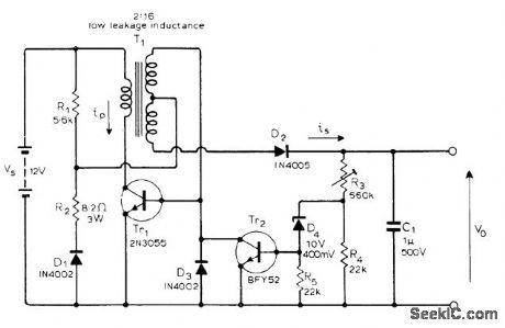
Conserves battery life by charging capacitor from 0 V at efficiencies over 80% and by allowing battery to be used to lower endpoint voltage, Will generate voltages above or below battery voltages. When used in capacitor-discharge ignition system, power conversion efficiency is so high that heatsink is unnecessary and only one power transistor is needed. Givesfull output voltage even when car battery voltage is less than half nominal value, as during cold starting. Article describes operation of circuit in detail. Tr1 may require series RC protection between collector and emitter.—R. M. Carter, Variable Voltage-Ratio Transistor Converter, Wireless World, Nov. 1975, p 519. (View)
View full Circuit Diagram | Comments | Reading(3048)
AUDIO_OPERATED_RELAY
Published:2009/6/30 2:05:00 Author:May
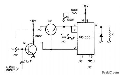
Addition of two general-purpose transistors to 555 timer gives audio-triggered relay that can be used for automatic recording of output of cttannel-monitorlng radio receiver or data from any audio link.Adjustable time delay R keeps control circuit actuated up to 5 s (determined by R and C) to avoid cycling relay during pauses in speech or dropouts in data. Q1 is NPN and Q2 is PNP. Attack time equals very short pullin time of 5-V reed relay K. Adjust 10K input pot just below point at which K pulls in when there is no audio input.-R. Taggart, Sound Operated Relay, 73 Magazine, Qct. 1977, p 114-11 (View)
View full Circuit Diagram | Comments | Reading(0)
DIFFERENTIAL_AMPLIFIE_RCLIPPER
Published:2009/6/30 2:04:00 Author:May
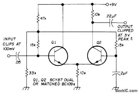
Provides gain as well as precise symmetrical clipping for improving intelligibility of speech fed into radio transmitter. Circuit reduces dynamic range of energy peaks to bdng them closer to average energy level. When inserted in series with microphone, use of clipper gives at least 6-dB increase in effective power. Signals are passed up to certain amplitude but limited above this level.-B. Kirkwood, Principles of Speech Pro-cessing, Ham Radio, Feb. 1975, p 28-34. (View)
View full Circuit Diagram | Comments | Reading(977)
12V_TO__11_V_WITH_CMOS_IC
Published:2009/6/30 2:04:00 Author:May
Bipolar inverter and rectifier together provide -11 V from 12-V auto battery for operating high-threshold MOS logic of portable or automotive equipment.Diode types are not critical. Inverter draws only about 1 mA from 12.V battery on standby and supplies 2 mA from -11V terminal.—B. Fette, Inexpensive Inverters Generate VGG for Portable MOS Applications, EDN|EEE Magazine, Dec. 15, 1971,p 51. (View)
View full Circuit Diagram | Comments | Reading(586)
HIGH_PASS_FILTER(HIGH_FREQUENCY)
Published:2009/6/30 2:04:00 Author:May
View full Circuit Diagram | Comments | Reading(619)
CIRCUIT_BREAKING_ALARM
Published:2009/6/30 2:04:00 Author:May
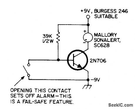
Operates from small 9-V battery, making it independent of AC power failure. Opening of switch or equivalent breaking of foil conductor removes ground from base of transistor, to energize alarm.-Circuits, 73 Magazine, April 1973, p 132. (View)
View full Circuit Diagram | Comments | Reading(813)
HIGH_PASS_ACTIVE_FILTER
Published:2009/6/30 2:03:00 Author:May
View full Circuit Diagram | Comments | Reading(0)
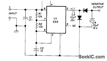
_6V_TO±15V
Published:2009/6/30 2:03:00 Author:May
Combination of 555 timer andtwo NE550A Precision adjustable regulators gives 0.1% line and load regulation,Timer operates as osdllator driving step-up transformer which feeds full-wave rectffier.— Signetics Analog Data Manual, signetics,Sunnyvale,CA,1977,p 726-727. (View)
View full Circuit Diagram | Comments | Reading(990)
60_dB_RANGE_FOR_AUDIO
Published:2009/6/30 2:03:00 Author:May
JFET acts as voltage-controlled resistor in peak-detecting control loop of 741 opamp. Input range is 20 mV to 20V, with response time of 1.2 ms and delay of 0.4.s.Outputisabout 1.4V P-P over entire 60-dB range,-N,Heckt、Automatic Gain Control Has 60~Decibel Range、Electronics,March 31,1977、p 107 (View)
View full Circuit Diagram | Comments | Reading(1242)
| Pages:1228/2234 At 2012211222122312241225122612271228122912301231123212331234123512361237123812391240Under 20 |
Circuit Categories
power supply circuit
Amplifier Circuit
Basic Circuit
LED and Light Circuit
Sensor Circuit
Signal Processing
Electrical Equipment Circuit
Control Circuit
Remote Control Circuit
A/D-D/A Converter Circuit
Audio Circuit
Measuring and Test Circuit
Communication Circuit
Computer-Related Circuit
555 Circuit
Automotive Circuit
Repairing Circuit