
Circuit Diagram
Index 1248
SWITCH_CLOSURE_COU_NTER
Published:2009/6/29 2:40:00 Author:May
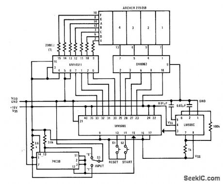
National MM5865 universal timer and counter chip is used with 74C00 debouncer and LM555C timer to drive digital display that counts closures of manual switch S3. Reset transition restores display to 0000. BCD segment outputs of MM5865 feed LED 4-digit display through MM14511 interface, whiledigit enable outputs go to display through DM8863 driver.— MOS/LSI Databook, National Semiconductor, Santa Clara, CA, 1977, p 2-23-2-32. (View)
View full Circuit Diagram | Comments | Reading(862)
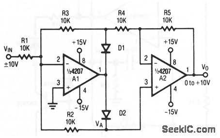
Precision_absolute_value_circuit
Published:2009/7/24 22:17:00 Author:Jessie

The values and types of D1 and D2 are not critical, but both diodes should be the same, and both must be able to withstand ±15 V (such as a 1N914). (View)
View full Circuit Diagram | Comments | Reading(1333)
Digitally_controlled_threshold_detector
Published:2009/7/24 22:16:00 Author:Jessie
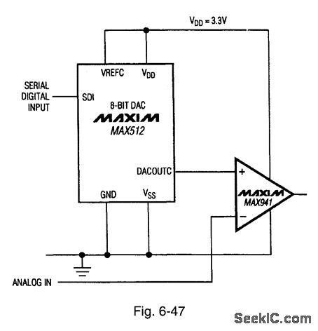
Figure 6-47 shows a MAX941 comparator combined with a MAX512 DAC to form a digitally controlled threshold detector. The analog signal to be compared is applied directly to the inverting input of the MAX941. The threshold point is set by the DAC output applied to the noninverting input. In turn, the DAC output is set by the serial digital input. As a result, the threshold can be set in eight discrete steps (depending on the serial input). MAXIM NEW RELEASES DATA BOOK, 1995, P. 3-69. (View)
View full Circuit Diagram | Comments | Reading(822)
High_stability_thermocouple_amplifier
Published:2009/7/24 22:16:00 Author:Jessie
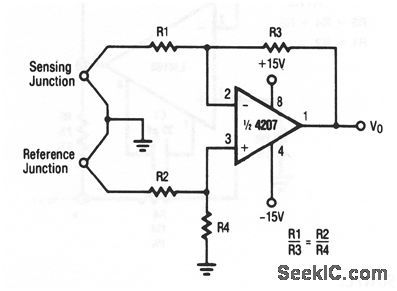

Notice that the reference-junction output is applied to the noninvert-ing input of the 4207, and the sensing-junction output is applied to the inverting input. See chapter 13 for additional temperature sensing and control circuits. (View)
View full Circuit Diagram | Comments | Reading(0)
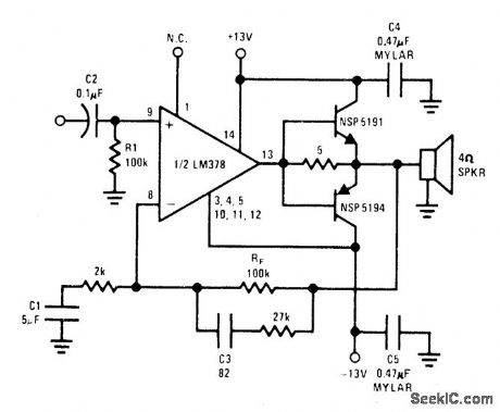
BRIDGE_AMPLIFIER
Published:2009/6/29 2:40:00 Author:May
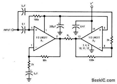
National LM377 dual power amplifieris used in bridge configurationto drive floating load that can be loudspeaker servomotor, or other device having impedance of 8 or 16 ohms,Maximum outputis 4 W at gain of 40 dB with 3-dB response extending fromabout 20 Hz to above 100 kHz.-″Audio Hand-book″ National Semiconductor、 Santa Clara、CA,1977、p 4-8-4-20. (View)
View full Circuit Diagram | Comments | Reading(0)
SIMPLE_TIME_DELAY
Published:2009/6/29 2:40:00 Author:May
View full Circuit Diagram | Comments | Reading(0)
Simple_line_transceiver
Published:2009/7/24 22:15:00 Author:Jessie
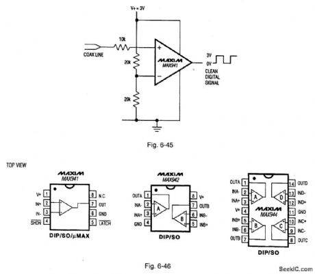
Figure 6-45 shows a MAX941 comparator connected as a simple line transceiver. The output is a clean square-wave signal at the input frequency. The output amplitude is equal to V+. See Fig. 6-46 for pin configurations. MAXIM NEW RELEASES DATA BOOK, 1995, P. 3-61, 3-69. (View)
View full Circuit Diagram | Comments | Reading(827)
12_W_WITH_BOOSTER_TRANSISTORS
Published:2009/6/29 2:40:00 Author:May

At signal input levels below 20 mW、National LM378 opamp suppliesload directly through 5-ohm resistor up to current peaks of about 100 mA。Above this level、booster transistors are biased on by load current through same resistor to increase output power, Transistors and opampmust have adequate heatsinks,-″Audio Hand-book″ National Semiconductor、Santa Clara、 CA,1977、p 442-4-43。 (View)
View full Circuit Diagram | Comments | Reading(1567)
Wien_bridge_oscillator_with_fed_amplitude_stabilization
Published:2009/7/24 22:14:00 Author:Jessie
This circuit is similar to that of Fig. 10-22, except that a lamp is not used, and the output is stabilized in amplitude by a 2N3819 FET. (View)
View full Circuit Diagram | Comments | Reading(1520)
WASHER_TIMER
Published:2009/6/29 2:39:00 Author:May
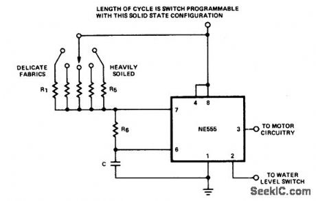
View full Circuit Diagram | Comments | Reading(710)
BOUNCELESS_SQUARE_OUTPUT
Published:2009/6/29 2:39:00 Author:May
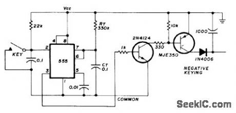
NE555 timer eliminates need for gates to suppress contact bounce. Timer can provide pulse at least 5 ms long (much longer if desired) and can remain on as long as trigger input (key pulse) is low (grounded). Timer triggers on negative-going edge of low-going pulse, such as key down to ground. Common negative is isolated from ground. VCC can be 5 to 15 VDC. Timer output can be connected directly to exciter keying input for negative grid keying. Because of square-wave output on make or break (100 ns each), circuits must be added in exciter or between keying transistors to provide at least 5-ms rise and fall times for Morse or RTTY key-ing.—B. Conklin, Improving Transmitter Keying, Ham Radio, June 1976, p 44-47. (View)
View full Circuit Diagram | Comments | Reading(651)
TIMER
Published:2009/6/29 2:39:00 Author:May
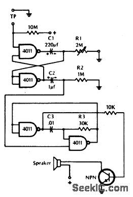
The timer can be used wherever time periods of up to seven minutes duration are needed. To turn on just touch the turn-on plate, and after the selected time has elapsed, an alarm will sound for a short period, then au-tomatically turn off. The turn-on touch plate, labeled TP in the diagram, is made up of two metal strips about 1/16-inch apart. Bridging the gap with your finger activates the timer. For more time range, increase RI and/or C1. R2 and C2 determine the period of time that the alarm will sound. Increasing either will extend the time. The tone of the alarm is determined by R3 and C3. Increasing either lowers the tone, decrqasing them raises the tone. (View)
View full Circuit Diagram | Comments | Reading(1093)
Low voltage bulb used in 220V power circuit diagram
Published:2011/8/1 2:21:00 Author:Ecco | Keyword: Low voltage bulb, 220V power
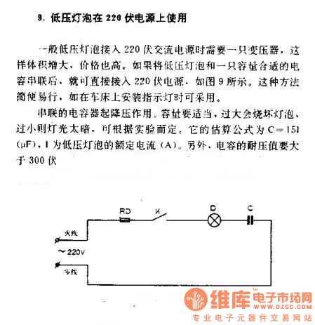
Low voltage bulb used in 220V power
Generally,the low-voltage light bulbsneeds a transformer when it is supplied by 220v AC power, then the volume increases, prices are high. If the low-voltage lamps and a suitable capacitor connect in series, they could access 220V power supply directly. According to figure 9, themethod is simple and easy, such as the installation of lights in the turning-lathe. Capacitors in series have the effect of reducing voltage. Thecapacitance should be appropriate, or burned out light bulbs when over, or the lighting is too dark when too small. It can be determined according to the experiment. Its estimating formula C = 15I (μF), I is the rated current of low-voltage lamp. In addition, the value of the capacitor voltage is greater than 300V. (View)
View full Circuit Diagram | Comments | Reading(1237)
HIGH_GAIN_JFET
Published:2009/6/29 2:38:00 Author:May
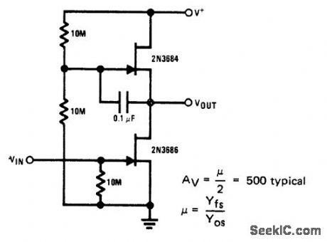
Simpletwo-JFET circuit provides gain of 500 at low power. Reducing drain cument increases gain at sacrifice of input dy-namic range.- FET Databook, National Semi-conductor, Santa Clara, CA, 1977, p 6-26-6-36. (View)
View full Circuit Diagram | Comments | Reading(1004)
741_TIMER
Published:2009/6/29 2:37:00 Author:May
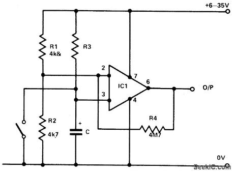
R1 and R2 hold the inverting input at half supply voltage. R4 applies feedback to increase the input impedance at pin 3. Pin 3, the nonin-verting input, is connected to the junction of R3 and C. Afterthe switch is opened, C charges via R3. When the capacitor has charged sufficiently for the potential at pin 3 to exceed that at pin 2 the output abruptly changes from 0 V to positive line potential. If reverse polarity operation is required, simply transpose R3 and C. R3 and C can be any values. Time delays from a frac-tion of a second to several hours can be ob-tained by judicious selection. The time delay-independent of supply voltage-is 0.7CR seconds where C is in farads. (View)
View full Circuit Diagram | Comments | Reading(1872)
LONG_INTERVAL_RC_TIMER
Published:2009/6/29 2:35:00 Author:May
View full Circuit Diagram | Comments | Reading(729)
90_W_PER_CHANNEL
Published:2009/6/29 2:33:00 Author:May
Combination of LM143 highvoltage opamp and curent booster can provide up to 90 WRMS into 4-ohm Ioudspeaker or 70 WRMS into 8-ohm Ioudspeaker. Circuit features indude shortcircuit and overload protection along with harmonic distortion below 0.1% at 1 kHz. Transistors Q1-Q4 should be on common Thermalloy 6006B or equivalent heat-sink.- Linear Applications, Vol. 2, National Semiconductor, Santa Clara, CA, 1976, AN-127, p 6-7. (View)
View full Circuit Diagram | Comments | Reading(916)
33_5_V_from_two_to_three_cells
Published:2009/7/24 23:16:00 Author:Jessie
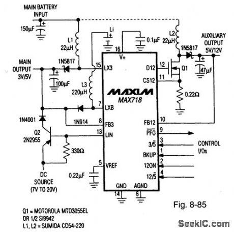
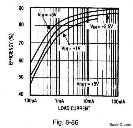
Figure 8-85 shows a MAX718 dual regulator connected to provide a maln 3.3-V/5-V output and an auxiliary 5-V/12-V output, with a 0.9-V to VOUT input range, and a start-up of 1.4 V Quiescent curren(VIN=3 V)is 140 μA for the main 5-V output.and 500 μA with both outputs. The maximum load-current capability of the malnsupply is 400 mA and 120 mA for the auxiliary Supply.Figure 8-86 shows theefficiency curves,The circuit can generate 3.3 V and 5 V, 3.3 V, and 12 V, or 5 V and 12 V, depending on the state of the logic inputs at pms 3 and 4.Two regulatedoutput voltages are generated from one of three input-voltage Sources∶an ac/dc wall-cube adapter(7 V or 20 V), a maln two-cell or three-cell battery,or a backuplithium battery. The dotted-line connection at the top of L2, which Powers theauxiliary supply, is normallv hard-wired to the maln battery,but it can also beconnected to the maln output when Power comes from the ac wall adapter. The main switching regulator automatically shuts off to save the batteries when the ac/dc wall cube is plugged in, MAXIM BATTERY MANAGEMENT CIRCUIT COLLECTION,1994, P.11. (View)
View full Circuit Diagram | Comments | Reading(717)
SIMPLE_TIMER
Published:2009/6/29 2:33:00 Author:May
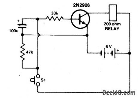
Press S1. The 100 μF electrolytic capacitor rapidly charges up at about 0.7 V. The transistor will be forward biased, and collector current will flow operating the relay. Release S1. The capacitor will begin to discharge via the 33 K resistor at the base of the transistor. When the voltage across the capacitor gets down to half a volt or so, the transistor base will no longer be forward biased, collector current will cease, and the relay will drop out. The capacitor will continue to discharge via the 47 K resistor. With the values shown, the relay will remain operated for about eight seconds. Long times are possible with lower values of capacitance by substituting a Darlington pair for the 2N2926. In this case, increase the two resitor values into the megohm range. (View)
View full Circuit Diagram | Comments | Reading(925)
Power_op_amp_with_parallel_output
Published:2009/7/24 23:14:00 Author:Jessie
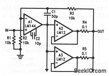
This circuit shows two LM12s (Fig. 10-46) connected in parallel to increase the load-current capability. (View)
View full Circuit Diagram | Comments | Reading(811)
| Pages:1248/2234 At 2012411242124312441245124612471248124912501251125212531254125512561257125812591260Under 20 |
Circuit Categories
power supply circuit
Amplifier Circuit
Basic Circuit
LED and Light Circuit
Sensor Circuit
Signal Processing
Electrical Equipment Circuit
Control Circuit
Remote Control Circuit
A/D-D/A Converter Circuit
Audio Circuit
Measuring and Test Circuit
Communication Circuit
Computer-Related Circuit
555 Circuit
Automotive Circuit
Repairing Circuit