
Circuit Diagram
Index 1243
12_V_AT_8_A
Published:2009/6/29 21:08:00 Author:May
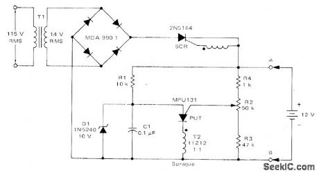
Charging circuit for lead-acid storage batteries is not damaged by short-circuits or by connecting with wrong battery polarity. Battery provides currentfor charging C1 in PUT relaxation oscillator. When PUT is fired by C1, SCR is turned on and applies charging current to battery. Battery voltage increases slightly during charge, increasing peak point voltage of PUT and making C1 charge to slightly higher voltage. When C1 vo!tage reaches that of zener D1, oscillator stops and charging ceases. R2 sets 12 V maximum battery voltage between 10 and 14 V during charge.-R. J. Haver and B. C. Shiner, Theory, Characteristics and Applications of the Programmable Unijunction Transistor, Moto-rola, Phoenix, AZ, 1974,AN-527, p 10. (View)
View full Circuit Diagram | Comments | Reading(2854)
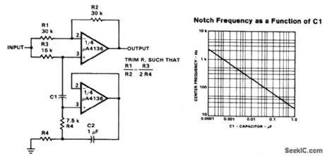
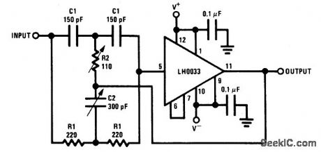
NOTCH_FILTER_USING_THE_μA4136_AS_A_GYRATOR
Published:2009/6/29 21:08:00 Author:May
View full Circuit Diagram | Comments | Reading(832)
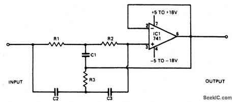
REJECTION_FILTER
Published:2009/6/29 21:07:00 Author:May
Circuit Notes
This narrowband filter using the 741 operational amplifier can provide up to 60 dB of rejection. With resistors equal to 100 K and capacitors equal to 320 pF, the circuit will reject 50 Hz. Frequencies within the 1 Hz to 10 kHz may be rejected by selecting components h accordance with the formula∶F=1/2πRCTo obtain rejections better than 40 dB,reslstors should be matched to 0.1%and capacitors to 1%. (View)
View full Circuit Diagram | Comments | Reading(884)
SOLAR_POWER_BACKUP
Published:2009/6/29 21:05:00 Author:May
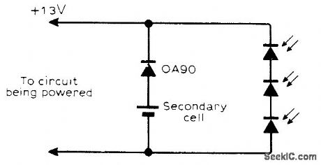
If solar-cell voltage drops 0.2 V below battery voltage, circuit is powered by storage cell feeding through forward-biased 0A90 or equivalent germanium diode. When solar-cell voltage exceeds that of battery, battery is charged by approximately constant reverse leakage current through diode. Battery can be manganese-alkaline type or zinc-silver oxide watch-type celL-M. Hadley Automatic Micropower Battery Charger, Wireless World, Dee. 1977, p 80. (View)
View full Circuit Diagram | Comments | Reading(986)
High_power_5_V_to_33_V_supply
Published:2009/7/24 22:58:00 Author:Jessie
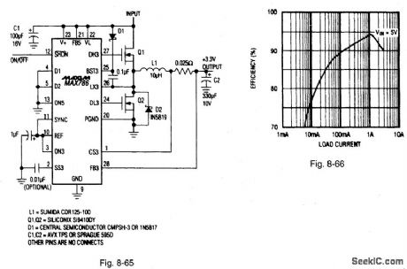
Figure 8-65 shows a MAX786 connected to provide 3.3 V from a 5-V supply. Figure 8-66 shows the efficiency curve. The circuit is suitable as a converter (possibly on a daughter card) to upgrade an existing desktop system with a new 3.3-V microprocessor. A synchronous rectifier is required. The input voltage range is 4.5 V to 6 V, with a quiescent current of 780 μA and a maximum load current capability (VIN = 4.5 V) of 3 A. MAXIM BAITERY MANAGEMENT CIRCUIT COLLECTION, 1994, P. 43.
(View)
View full Circuit Diagram | Comments | Reading(607)
SCSI_terminal_power_protection
Published:2009/7/24 22:56:00 Author:Jessie

Figure 8-64 shows how an LTC1153 can be used to protect the termination power for an SCSI (small computer serial interface) circuit. With the values shown, the dc current is limited to 1 A with a trip-delay time of 1 ms. The breaker trips if the cable or connector is accidentally shorted and will retry every second until the short circuit is removed. The termination power then returns to normal, and the interface is reconnected. The microprocessor can continuously monitor the status of the termination power (via the STATUS pin) and take further action if the fault condition persists. A gate-voltage ramp is slowed to smoothly start large capacitive loads (soft start). The circuit also includes a power-supply filter to ensure that the supply (VS) is maintained above 3.5 V until the gate is fully discharged during a short circuit. LINEAR TECHNOLOGY, APPLICATION NOTE 53, P. 16. (View)
View full Circuit Diagram | Comments | Reading(698)
Simple Crystal Oscillator Test Circuit
Published:2011/7/22 22:16:00 Author:Joyce | Keyword: Simple, Crystal Oscillator , Test
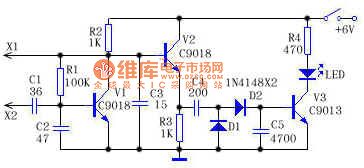
Here is an introduction of a simple crystal oscillation test machine, whose schematic circuit is as shown in the figure attached.
In the figure, V1 and its peripheral components (including the crystal oscillator to be tested) compose a capacitance connecting three point type oscillator. When the two ends of probe X1 X2 are connected with the crystal oscillator to be tested, the circuit will start oscillation. Oscillation signal will be output after being amplified by the emitter follower V2. Then it will provide bias current to V3 after being coupled by C4 and voltage-multiplied and rectificated by D1, D2. So V3 will break over and LED will flicker. If the crystal oscillation doesn`t work well or disconnects, the circuit will not start oscillation and LED will not flicker. (View)
View full Circuit Diagram | Comments | Reading(896)
Fast_half_wave_rectifier
Published:2009/7/24 22:54:00 Author:Jessie
This circuit provides rectification with 1% accuracy from dc to 100 kHz, with a slew rate of 10V/μs. Operation can be extended to full-wave rectification as shown in Fig. 10-40. (View)
View full Circuit Diagram | Comments | Reading(1631)
Electronic_circuit_breaker
Published:2009/7/24 22:54:00 Author:Jessie
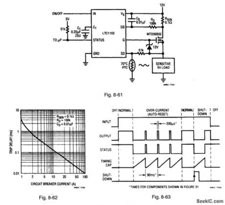
Figure 8-61 shows an LTC1153 connected for thermal shutdown. Figures 8-62 and 8-63 show the characteristics and timing diagram, respectively. The LTC1153 interrupts power to a sensitive load in the event of an overcurrent condition, and remains tripped for a period of time programmed by external capacitor CT. The switch is then automatically reset, and the load is momentarily reconnected. If the load current is still too high, the switch is shut down again. This cycle continues until the overcurrent condition is removed, thus protecting both the sensitive load and the power MOSFET. Dc trip current is set by RSEN at 1 A. The trip-delay time is set by RD and CD, and is shorter for increasing current (similar to a mechanical circuit breaker), as shown in Fig. 8-62. The circuit breaker is automatically reset (retried) every 200 ms until the overload is removed. An open-drain STATUS output warns the host microprocessor whenever the circuit is tripped. A shutdown (SD) input interfaces with a PTC thermistor to sense overtemperature conditions (over 70°C) and trip the circuit breaker. LINEAR TECHNOLOGY, APPLICATION NOTE 53, P. 15, 16.
(View)
View full Circuit Diagram | Comments | Reading(0)
Precision_clamp
Published:2009/7/24 22:53:00 Author:Jessie
In this circuit, the output is precisely clamped from going more positive than the reference voltage, preventing the op amp from saturating when D1 is reverse biased. (View)
View full Circuit Diagram | Comments | Reading(1054)
BATTERY_MONITOR
Published:2009/6/29 21:02:00 Author:May
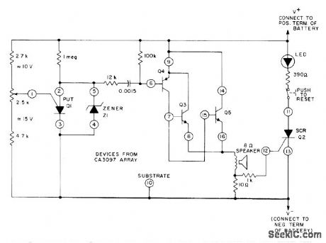
Uses CA3097 transistor array to provide active elements required for driving indicators serving as aural and visual warnings of low charge on nicad battery. LED remains on until circuit is reset with pushbutton switch.- Circuit Ideas for RCA Linear ICs, RCA Solid State Division, Somerville, NJ, 1977, p 9. (View)
View full Circuit Diagram | Comments | Reading(0)
BULK_NICAD_CHARGER
Published:2009/6/29 20:59:00 Author:May
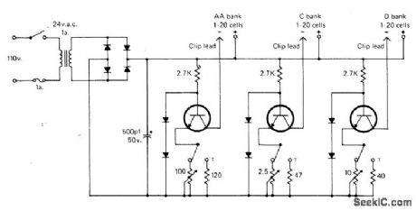
Can handle up to 20 AA cells, 20 C cells, and 20 D cells simultaneouslt, with charging rate determined separately for each type. Single transfrmer and fullwave rectifier feed about 24 VCD to three separate regulators. AA-cell regulator uses 100-ohm resistor to vary charge rate from 6 mA to above 45 mA, C-cell chargerate range is 24 to 125 mA, and D-cell range is 60 to 150 mA. Batteries of each type should be about same state of discharge. Batteries are recharged in series to avoid need for separate regulator with each cell. Tricklecharge switches cut charge rates to about 2% of rated normal charge (5 mA for 500-mAh AA cells).Transistors are 2N4896 or equivalent. Use heatsinks. All diodes are 1N4002.-J.J. Schultz, A Bull Ni-Cad Recharger, CQ, Dec. 1977, p 35-36 and 111. (View)
View full Circuit Diagram | Comments | Reading(844)
High_side_switches_for_33_Voperation
Published:2009/7/24 22:52:00 Author:Jessie
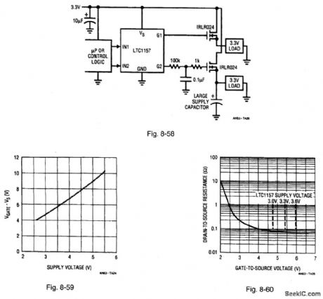
Figure 8-58 shows an LTC1157 connected to provide high-side switching (Chapter 2) for two 3.3-V loads. Figure 8-59 shows the gate-voltage (above supply) characteristics for the LTC1157, which is a dual, low-voltage MOSFET driver specifically designed for operation between 2.7 V and 5.5 V The LTC1157 internal charge pump boosts the gate-drive voltage 5.4 V above the 3.3-V positive supply (or 8.7 V above ground). This voltage fully enhances a logic-level N-channel below 4.6 V, and housekeeping is performed (data storage, etc.) before the batteries are completely discharged. The other three channels of the LTC 1156 act as switches (under microprocessor control) to power the remaining sections of the computer. The number of switches can be increased by adding more LTC1155 or LTC1156 circuits as needed. LINEAR TECHNOLOGY, APPLICATION NOTE 53, P. 11. (View)
View full Circuit Diagram | Comments | Reading(772)
HIGH_Q_NOTCH_FILTER
Published:2009/6/29 20:58:00 Author:May

Circuit NotesA shows atwin-T network connected to anLM102 to form a high Q, 60 Hz notch filter, Thejunction of R3 and C3, which t normally connected to ground, is bootstrapped to the outputof the follower, Because the output of the follower is a very low impedance, neither the depth nor the frequency of then.tch change; however, the Q is raised In proportion to thealηount of signal fed back to R3 and C3. Bshows the response ofa normal twin-T and theresponse with the foilower added. (View)
View full Circuit Diagram | Comments | Reading(0)
45_MHz_NOTCH_FILTER_
Published:2009/6/29 20:56:00 Author:May
Circuit NotesComponenc value sensitivity is extremely critical, as are temperature coefficients and matching ofthe components. Best performa,ce is attained when perfectly matched components are used and when the gain of the amplifier is unity.To illustrate,the quality factor Q is very high as amplifier gam approaches1 with all components matched(In fact,theoretically it approaches co)but decreases toabout 12.5 with the amplifier gain at 0.98. (View)
View full Circuit Diagram | Comments | Reading(709)
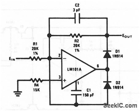
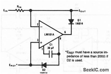
Precision_diode
Published:2009/7/24 22:51:00 Author:Jessie
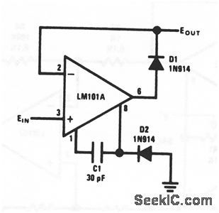
This circuit virtually eliminates diode threshold potential so that millivolt signals can be rectified、Less than 100μV change at the input causes the output of the LM101A to swing from negative to positive. (View)
View full Circuit Diagram | Comments | Reading(817)
CHARGING_SILVER_ZINC_CELLS
Published:2009/6/29 20:52:00 Author:May
Used for initial charging and subsequent rechargings of sealed dry-charged lightweight cells developed for use in missiles, torpedoes, and space applications. Article covers procedure for filling cell with potassium hydroxide electrolyte before placing in use (cells are dry-charged at factory and have shelf life of 5 or more years in that condition). Charge current should be 7 to 10% of rated cell discharge capacity; thus, for Yardney HR-5 cell with rated discharge of 5 A, charge at 350 to 500 mA. Stop charging when cell voltage reaches 2.05V.If used only for battery charging, large filter caacitor can be omitted.-S.Kelly, Will Silver-Zinc Replace the Nicad?, 73 Magazine, Holiday issue 1976, p 204-205. (View)
View full Circuit Diagram | Comments | Reading(674)
Op_amp_bridge_amplifier
Published:2009/7/24 22:50:00 Author:Jessie
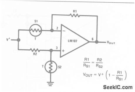
In this circuit, the LM107 serves as the amplifier for two temperature sensors connected In a bridge configuration. As shown by the equations, VOUT depends on the resistance of the sensors. In turn, sensor resistance depends on temperature, so VOUT is related to temperature. See chapter 13 for additional temperature sensing and control circuits. (View)
View full Circuit Diagram | Comments | Reading(717)
12_V_FOR_NICADS
Published:2009/6/29 20:47:00 Author:May
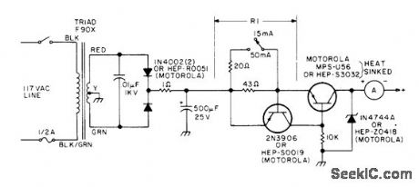
Produces constant current with simple transistor circuit, adjustable to 15 or 50 mA with switch and R1. Zener limits voltage at end of charge. Developed for charging 10-cell pack having nominal 12.5V, as used in many transceivers.-H. Olson, Battery Chargers Exposed, 73 Magazine, Nov.1976, p 98-100 and 102-104. (View)
View full Circuit Diagram | Comments | Reading(845)
Bar_graph_level_gauge
Published:2009/7/24 22:14:00 Author:Jessie
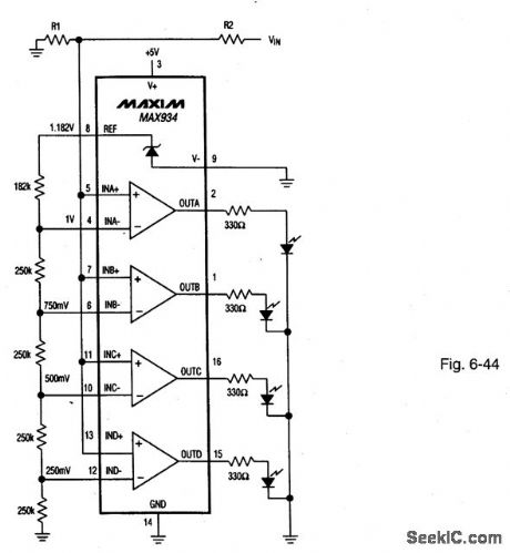
Figure 6-44 shows a MAX934 connected as a simple, four-stage level detector with LED readouts. The full-scale threshold (all LEDs on) is given by VIN=(R1 + R2)/R1 volts. The other thresholds are at 3/4 full-scale, 1/2 full-scale, and 1/4 full-scale. The output resistors limit the current into the LEDs. MAXIM NEW RELEASES DATA BOOK, 1995, P. 3-58. (View)
View full Circuit Diagram | Comments | Reading(1557)
| Pages:1243/2234 At 2012411242124312441245124612471248124912501251125212531254125512561257125812591260Under 20 |
Circuit Categories
power supply circuit
Amplifier Circuit
Basic Circuit
LED and Light Circuit
Sensor Circuit
Signal Processing
Electrical Equipment Circuit
Control Circuit
Remote Control Circuit
A/D-D/A Converter Circuit
Audio Circuit
Measuring and Test Circuit
Communication Circuit
Computer-Related Circuit
555 Circuit
Automotive Circuit
Repairing Circuit