
Circuit Diagram
Index 1259
Analog_multiplier
Published:2009/7/25 0:05:00 Author:Jessie
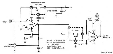
This circuit shows an LTC1043 (Fig. 1-4B) connected to form a high-precision (0.01%) analog multiplier. The LTC1043 clock is common to both sections, so the X and Y inputs are synchronized. To calibrate, short the X and Y inputs to 1.7320 V and trim for a 3-V output. (View)
View full Circuit Diagram | Comments | Reading(0)
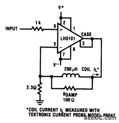
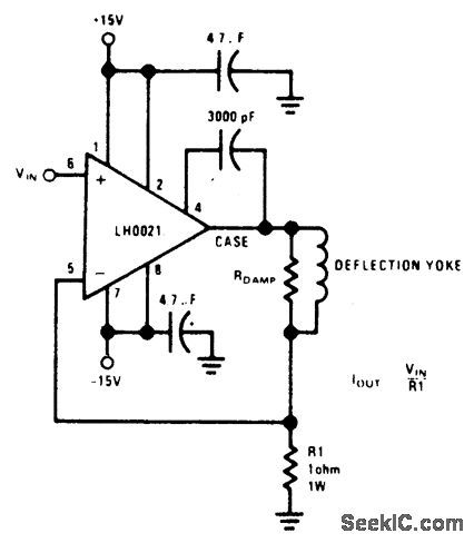
CRT_DEFLECTION_YOKE_DRIVER_
Published:2009/6/28 23:57:00 Author:May
View full Circuit Diagram | Comments | Reading(874)
Simple illumination photometry instrument circuit diagram
Published:2011/7/28 4:44:00 Author:Sophia | Keyword: Simple illumination photometry instrument
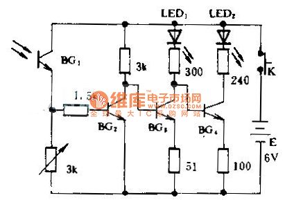
When the outside light is dark, the photodiode BG1 shows large resistance and allows small current. So, BG2 ends, BG2 connects, LED1 lights.
When the light is bright, BG1 outputs strong current, so that BG2 can be in the saturation, BG3 ends and BG4 connects, LED1 is off and LED2 (red) lights.
When the light is normal, three transistors are in amplified state. two LEDs emit dim light.
(View)
View full Circuit Diagram | Comments | Reading(737)
HIGH_IMPEDANCE_METER_DRIVER_
Published:2009/6/28 23:56:00 Author:May
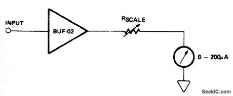
View full Circuit Diagram | Comments | Reading(774)
Timer_one_shot_monostable
Published:2009/7/25 0:03:00 Author:Jessie
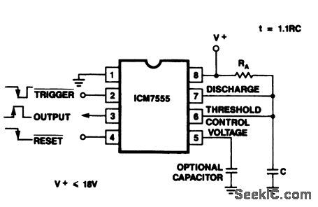
This circuit shows an ICM7555/56 timer connected as a one-shot or monostable multivibrator. The output time is determined by 1.1RAC. Use high values of R and low values of C for minimum current drain. At a supply of 4.5 V, this circuit will drive at least two TTL loads. The waveforms at pins 2, 3, and 4 show the relationships of the trigger, output and reset signals. (View)
View full Circuit Diagram | Comments | Reading(714)
96_V_AT_20_mA
Published:2009/6/28 23:53:00 Author:May
Developed to charge 200-mAh nickel-cadmium batteries for two transceivers simultaneously. Batteries will be fully charged in 14 hours, using correct 20-mA charging rate. Zone diode ensures that voltage cannot exceed safe value if battery is accidentally disconnected while under charge. Diode types are not critical.-D. A. Tong,A Pocket V.H.F. Transceiver, Wireless World, Aug, 1974 p 293-298. (View)
View full Circuit Diagram | Comments | Reading(811)
HIGH_SPEED_LINE_DRIVER_FOR_MULTIPLEXERS
Published:2009/6/28 23:49:00 Author:May
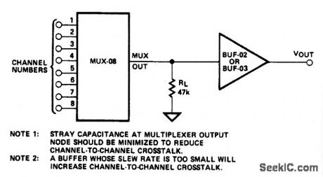
View full Circuit Diagram | Comments | Reading(743)
Timer_multivibrator_with_adjustable_duty_cycle
Published:2009/7/25 0:01:00 Author:Jessie
This circuit shows an ICM7555/56 timer connected as a free-running multivibrator, with an adjustable duty cycle, The frequency is determined by 1.44(RA + 2RD)C, while the duty cycle is set by RB/(RA + 2RB). Use high values of R and low values of C for minimum current drain. At a supply of 4.5 V, this circuit will drive at least two TTL loads. (View)
View full Circuit Diagram | Comments | Reading(866)
TIMER_FOR_WIPER
Published:2009/6/28 23:49:00 Author:May
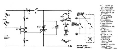
Provides automatic one-shot swipes at preselected intervals from 2 to 30 s for handling mist, drizzle, or splash from wet road. Circuit shorts out homing switch inside windshield-wiper mptor, which is usually in parallen with slow-speed contacts of wiper dashboard switch terminals at a time to find pins that shatr wiper. When blades begin moving, remove jumper; blades should then finish sweep and shut off. It is these terminals of switch that are connected to points A and B of control circuit.-V. Mele, Mist Switch-It's for Your Windshield Wipers, Popular Science, Aug.1973, p 110. (View)
View full Circuit Diagram | Comments | Reading(762)
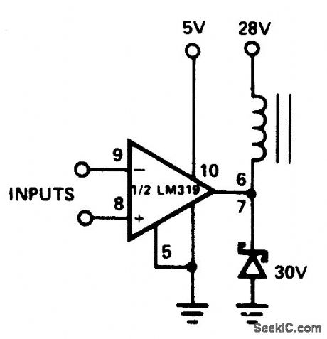
5_V_CLAMPED_COMPARATOR
Published:2009/6/28 23:48:00 Author:May
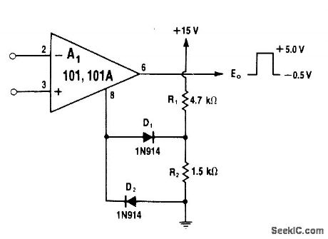


R1 and R2 provide +3.8V bias for D1,clamping positive outputof comparator opamp to +5 V,D2 limits negative output swing to-0.5V.Open-loop circuit means that output voltage will vary in proportion to load current.—W.G.Jung, IC Op-Amp Cookbook, Howard W.Sams,Indianapolis,IN、1974,p 226-228 (View)
View full Circuit Diagram | Comments | Reading(659)
BIFET_CABLE_DRIVER
Published:2009/6/28 23:48:00 Author:May

View full Circuit Diagram | Comments | Reading(675)
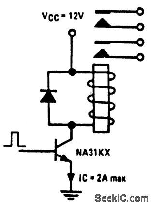
RELAY_DRIVER__
Published:2009/6/28 23:46:00 Author:May
View full Circuit Diagram | Comments | Reading(784)
CROSSOVER_FOR_20_Hz_SUBWOOFER
Published:2009/6/28 23:44:00 Author:May
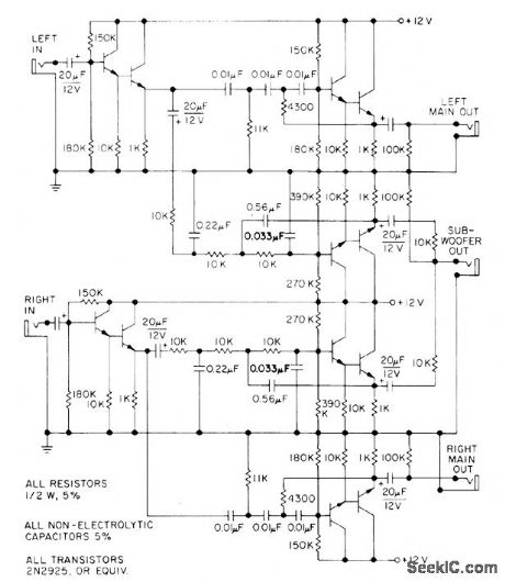
Used at channel outputs of stereo system when re-producing music down to 20 Hz as synthesized by electronic function generators. Active crossover network drives subwoof er (low-bass loudspeaker) connected in bridgedcenter configu-ration, for handling sounds below range of normal woofer. Crossover consists of thirdorder Butterworth (18 dB per octave) networks providing 20-Hz cutoff along with 100-Hz cross-over. Response of subwoofer should extend one octave above crossover. 0ne advantage of active crossover is freedom from transient intermodulation distortion.-W. J. J. Hoge, Switched-0n Bass, Audio, Aug. 1976, p 34-36, 38, and 40 (View)
View full Circuit Diagram | Comments | Reading(2399)
HIGH_INPUT_IMPEDANCE
Published:2009/6/28 23:43:00 Author:May
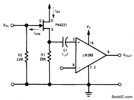
Use of JFET as isolator boosts input impedance of opamp to 22 megohms for low-frequency input signals.Impedance drops to 3.9 megohms as frequency increases to about 20 kHz. Overall gain of circuit is about 45 dB when using 18-V supply.- Audio Handbook, National Semiconductor, Santa Clara, CA, 1977, p 4-21-4-28. (View)
View full Circuit Diagram | Comments | Reading(0)
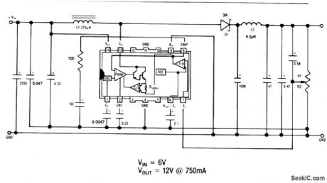
Adjustable_dc_dc_step-down_converter5_A
Published:2009/7/25 1:14:00 Author:Jessie
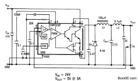
This circuit shows an LAS-6350/6450 used as a step-down converter with an adjustable output. (View)
View full Circuit Diagram | Comments | Reading(609)
46_dB_GAlN
Published:2009/6/28 23:43:00 Author:May
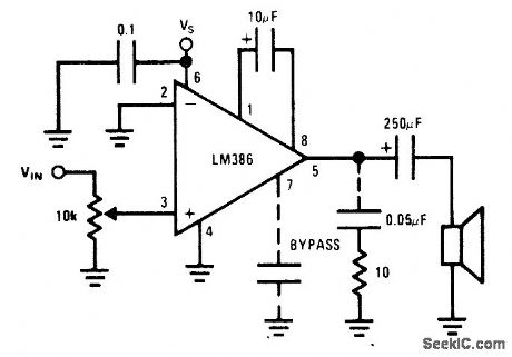
Single National LM386 power amplifier provides gain of 200 V/V at maximum output power of 250 mW for 12-V supply. Op-tional 0.05-μF capachor and 10-ohm resistor suppress bottomside oscillation occurring during negative swing into Ioad drawing high current.- Audio Handbook, National Semicon-ductor, Santa Clara, CA, 1977, p 4-30-4-33. (View)
View full Circuit Diagram | Comments | Reading(651)
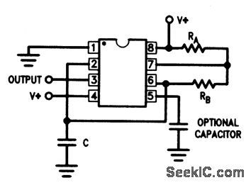
Adjustable_dc_dc_step_up_converter_1_A
Published:2009/7/25 1:13:00 Author:Jessie
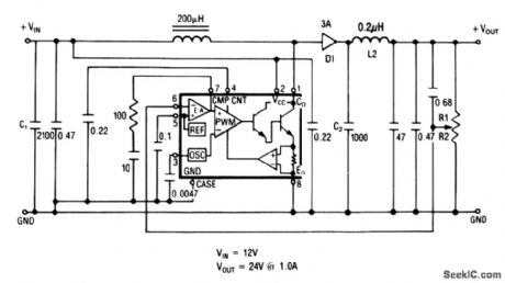
This circuit shows an LAS-6330/6430 used as a step-up converter with an adjustable output. (View)
View full Circuit Diagram | Comments | Reading(671)
Adjustable_dc_dc_step_down_converter_3_A
Published:2009/7/25 1:12:00 Author:Jessie
This circuit shows an LAS-6350/6450 used as a step-down converter with an adjustable output. (View)
View full Circuit Diagram | Comments | Reading(772)
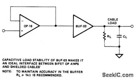
CAPACITIVE_LOAD_DRIVER
Published:2009/6/28 23:42:00 Author:May
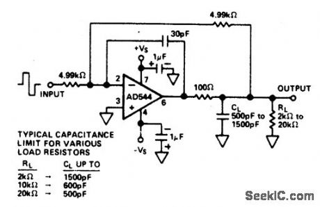
View full Circuit Diagram | Comments | Reading(832)
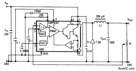
Adjustable_dc_dc_step_up_converter_750_mnA
Published:2009/7/25 1:11:00 Author:Jessie
This circuit shows an LAS-6320P used as a step-up converter with anadjustable output. (View)
View full Circuit Diagram | Comments | Reading(724)
| Pages:1259/2234 At 2012411242124312441245124612471248124912501251125212531254125512561257125812591260Under 20 |
Circuit Categories
power supply circuit
Amplifier Circuit
Basic Circuit
LED and Light Circuit
Sensor Circuit
Signal Processing
Electrical Equipment Circuit
Control Circuit
Remote Control Circuit
A/D-D/A Converter Circuit
Audio Circuit
Measuring and Test Circuit
Communication Circuit
Computer-Related Circuit
555 Circuit
Automotive Circuit
Repairing Circuit