
Circuit Diagram
Index 1494
GuangZhou HONDA Fit saloon car engine circuit 9
Published:2011/7/11 2:36:00 Author:TaoXi | Keyword: GuangZhou, HONDA, Fit, saloon car, engine circuit
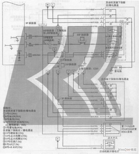
GuangZhou HONDA Fit saloon car engine circuit
Fuse:
Engine room under-cover fuse/relay box
1. Number 3 IG(50A)
2. Number 6 MAIN(50A)
3. Number 8 spare(10A)
4. Number 16 STOP HORN(15A) (Right side of the cab: 10A)
5. Number 1 storage battery(80A)
The fuse/relay box below the instrument panel
6. Number 11 fuel pump(15A)
7. Number 14 ignition coil 1 (15A)
8. Number 15 ignition coil 2 (15A)
9. Number 17 meter(7.5A)
10. Number 1 A/C(7.5A)
11. Number 8 +B IGP(15A) (View)
View full Circuit Diagram | Comments | Reading(939)
The Multi-purpose signal generator circuit
Published:2011/7/14 22:16:00 Author:TaoXi | Keyword: Multi-purpose, signal generator
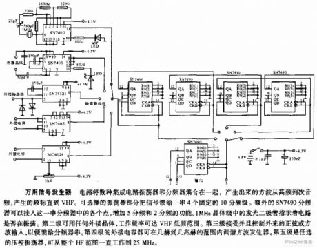
The multi-purpose signal generator circuit is composed of the integrated circuit oscillators and the frequency dividers, it produces the square wave from the high frequency to the sub-audio frequency, and it also produces the frequency standard VHF. The alternative oscillator part feeds the signal back to the 10-frequency divider stage. The extra SN7490 frequency divider can connect into the points of the frequency divider to add the 5 frequency division and 2 frequency division functions. The light-emitting diode of the 1MHz crystal stage indicates that whether the circuit is oscillating. The second stage can use any external crystal, the operating frequency is in the VHF low frequency range.
(View)
View full Circuit Diagram | Comments | Reading(1445)
The Digital programmable amplifier circuit
Published:2011/7/11 2:24:00 Author:TaoXi | Keyword: Digital, programmable amplifier
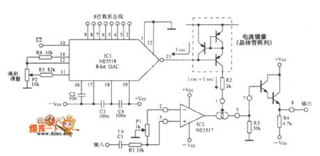
The Digital programmable amplifier circuit is as shown in figure:
(View)
View full Circuit Diagram | Comments | Reading(745)
The Wide dynamic range gain control amplifier circuit
Published:2011/7/11 2:25:00 Author:TaoXi | Keyword: Wide dynamic range, gain control, amplifier circuit
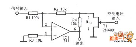
The Wide dynamic range gain control amplifier circuit is as shown in the figure:
(View)
View full Circuit Diagram | Comments | Reading(776)
Anti-jamming Circuit Principle Diagram with Four Analog Input Channels
Published:2011/7/12 3:32:00 Author:Michel | Keyword: Analog Input Channels, Anti-jamming Circuit, Principle Diagram
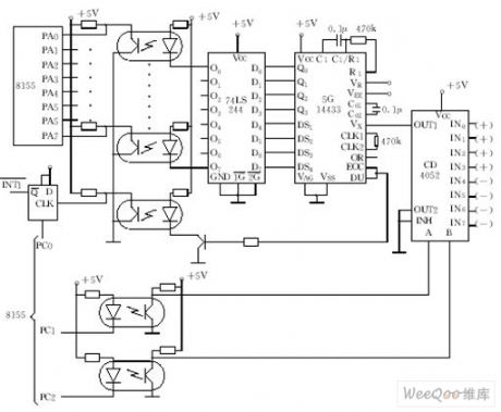
Switch input/output channels and analog input and output channels and they are interference enter channels.The object and input/output public ground lines should be removed and interference pulse should be suppressed by realizing electrical isolati to cut off this channel.The most common isolation device is photoelectric couplers, its internal structure is shown as the above picture.
Anti-jamming Circuit Principle Diagram with Four Analog Input Channels
We have to notice that:When we use photoelectric couplers to isolate input output channel,all signals(digital quantity signals,control signal,condition siganl) should be isolated and it makes both sides isolation have no electrical ties.Otherwise,the isolation is meaningless.
(View)
View full Circuit Diagram | Comments | Reading(1605)
The SIPMOS transistor push-pull control circuit
Published:2011/7/11 2:25:00 Author:TaoXi | Keyword: SIPMOS, transistor, push-pull, control
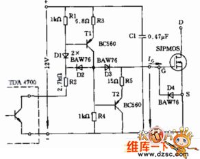
Figure:The SIPMOS transistor push-pull control circuit
(View)
View full Circuit Diagram | Comments | Reading(697)
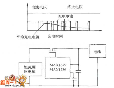
Charging circuit composed of the MAXl678/MAXl736
Published:2011/7/11 2:24:00 Author:TaoXi | Keyword: Charging circuit
View full Circuit Diagram | Comments | Reading(575)
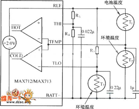
MAX712/MAX713 temperature control typical circuit
Published:2011/7/11 2:24:00 Author:TaoXi | Keyword: temperature control, typical
View full Circuit Diagram | Comments | Reading(648)
Transistor DC/DC Converter Circuit
Published:2011/7/13 8:24:00 Author:Michel | Keyword: DC/DC Converter Circuit
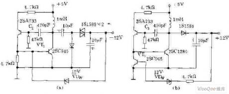
The above picture is a small power DC/DC converter circuit composed of transistor.Picture (a) is the circuit which turns +5V input voltage to -12V output voltage.Picture (b) is the circuit which turns +5V input voltage to +12V output voltage.For any circuit,it's feedback to driving transistor VT1 if the output voltage exceeds voltage regulator tube VDw,which keeps stable output voltage.Thus, output voltage is equal to stable voltage of the voltage regulator tube.And the output voltage can be adjusted if the stble voltage is changed.It works if the capacitance C1 value is changed when the circuit does not oscillate.The output current is 15~20mA,voltage stablity is around 5% and the efficiency is 80%~90%. (View)
View full Circuit Diagram | Comments | Reading(3800)
555 audio equipment turn-on and turn-off
Published:2011/7/11 23:08:00 Author:TaoXi | Keyword: 555, audio equipment, turn-on, turn-off,
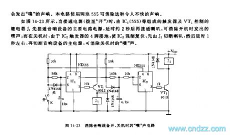
When you are tuning on or tuning off the audio equipment, the audio equipment circuit has the process from the temporary stabilization state to the stabilization state, so the speaker will send out the sound of pu , this circuit can eliminate this sound by using two pieces of 555.
As the figure 14-23 shows, when the power supply turns on, the trigger which is composed of the IC1(555) and the relay J1 which is controlled by VT1 are connected to the main circuit power of the audio equipment, the delay time is about 2 seconds and then connect the speaker, so the sound of pu when you are tuning on the equipment is eliminated; when you are tuning off the equipment, because the pin-4 of the trigger IC2 is connected with the ground, so the IC2 resets, and it firstly cuts off the speaker through J2, the delay time is about 1 second, then it cuts off the main power of the audio equipment, so the sound of pu is eliminated.
(View)
View full Circuit Diagram | Comments | Reading(585)
5V/1A Constant AC Stabilized Voltage Power Supply Circuit
Published:2011/7/13 7:25:00 Author:Michel | Keyword: 5V/1A, Constant AC , Stabilized Voltage, Power Supply Circuit
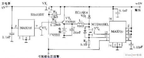
The above picture is 5V/1A constant AC stabilized voltage power supply circuit.The circuit can still provide 5V/1A power supply in 80 minutes when 5V main power supply is off.MAX709 is monitoring circuit and the feet 7 outputs high PWL and transistor VT is in conduction state when its feet 2 monitors main power supply.The DC/DC converter MAX720 is in shut-off mode and VT1 and VT2 charge batteries.Feet 7 outputs low PWL and VT2 and VT3 stop and MAX720 is in work mode and constant power output increases to 5V when main power supply decreases to MAX709 offsetting threshold level(typical value is 4.65V). (View)
View full Circuit Diagram | Comments | Reading(1543)
Small Power Uninterrupted Power Supply Circuit
Published:2011/7/13 7:24:00 Author:Michel | Keyword: Small Power, Uninterrupted, Power Supply Circuit
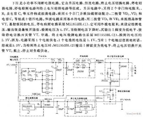
The above picture is a small power uninterrupted power supply circuit.It consists of lift circuit, constant current circuit, terminate circuit, switching circuit, power switching circuit, power switching circuit, power detection circuit and termination voltage detection circuit etc.In the lift circuit,the two longest-serving outfield and resistance R2, R1and capacitance C1 constitute oscillating circuit and it uses six longest-serving outfield in parallel way to strengthen the drive ability.Diode VD1 and VD2 and capacitance C2 constitute 2 times voltage circuit.Constant current circuit uses basic circuit, diode VD3 and VD4 to offset voltage between the transistor VT1 and basic emitting.The blackout detection circuit, M5193BL (1) can use set the external resistance,R3 to set detecting voltage and the output is a very open type, detection set voltage is 4.5 V. (View)
View full Circuit Diagram | Comments | Reading(650)
Automatic charging, power supply dual-use device circuit (2)
Published:2011/7/14 22:17:00 Author:TaoXi | Keyword: Automatic, charging, power supply, dual-use, device circuit

Operating principle:
The circuit is as shown in figure 4-3, this device uses three pieces of integrated circuits: IC1 is the LM317, the adjustable voltage stabilization power supply is composed of LM317 and other surrounding components, the adjustment range is 1.25V-15V; IC2 is the pulse oscillator which is composed of the time base circuit 555, the duty ratio is 60%; IC3 is the high current and low current charging and discharging conversion control circuit.
After you pressing the button AN, the battery voltage is lower than the gate voltage of D, so D outputs the high level, the transistor V4 conducts, the relay K closes to form the self-protection.
(View)
View full Circuit Diagram | Comments | Reading(580)
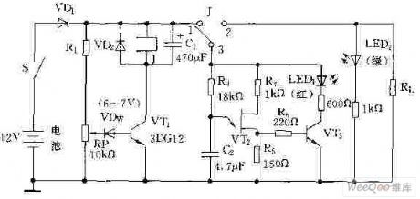
The Automatic charger circuit
Published:2011/7/21 0:55:00 Author:TaoXi | Keyword: Automatic, charger circuit

Automatic charger circuit
The automatic charger circuit which is composed of the VT1 charging circuit and the LM324 control circuit is as shown in figure 2-23, the charging loop is composed of the VD1, VD2, R5, VT1 and the batteries, the charging current is the pulsating current, it is controlled by the R5. The LM324 is the voltage comparator, the in-phase port has the comparison voltage and it is set by the potentiometer RP; the reverse phase voltage value is decided by the number of the rechargeable batteries, for example, when you are charging 2 nickel cadmium batteries, the comparison voltage can be set to 3V. The reverse phase pin-2 of LM324 is connected with the battery positive port through the resistor R4.
The power supply of LM324 is composed of VD2 and C1.
(View)
View full Circuit Diagram | Comments | Reading(1211)
Battery Discharging Control Indication Circuit
Published:2011/7/13 7:24:00 Author:Michel | Keyword: Battery, Discharging Control, Indication Circuit
The above picture is battery discharging control indication circuit and its overdischarging circuit is composed of R1,RP and VDw.R3,C2,VT2 and VT3 constitute overdischarging indication circuit.Battery voltage R1 and RP division voltage break down VDw,which make the VT2 getfull and conduct and the 1.3 openning touch point conducts and overlaod R1 works when the switch turns on.R1 and RP can not break down VDw,which can not make VT1 get full and condcut and the relay stops working when the battery voltage decreases to 10~10.5V. (View)
View full Circuit Diagram | Comments | Reading(807)
12V/6A charging circuit with excellent charge curve and auto-cutout circuit
Published:2011/7/21 0:54:00 Author:TaoXi | Keyword: 12V/6A, charging circuit, excellent charge curve, auto-cutout circuit
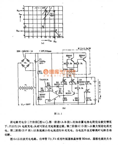
The charging process of this circuit is divided into three stages (figure a): stage one, when the storage battery has no residual electric charge, you can charge the battery with 2A current to prevent the overload of the charging device. Stage 2 (C-D), you need to charge the battery with the largest constant current. Stage 3 (E-F), you need to charge the battery with rapid decreasing current. When the voltage is high enough, the circuit will cut off automatically.
Figure b is the charging circuit. The power tubes T2 and T3 use the epitaxy base electrode transistor BD646, the base electrode current has relationship with the load current.
(View)
View full Circuit Diagram | Comments | Reading(1532)
Constant current-constant voltage dual-function charger circuit
Published:2011/7/18 21:51:00 Author:TaoXi | Keyword: Constant current, constant voltage, dual-function, charger
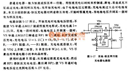
The ordinary charger has the single function of the constant current charging or constant voltage charging. The circuit is as shown in figure 5-17. When the charging begins, the voltage of the battery istoo low to conduct the VS, the LM317 is connected into the form of constant current charging, the charging current I=1.25/R. When the voltage of battery invreases to the certain value, VS conducts, the pin-1 of LM317 is connected with the ground through the RP1 and VS, at this time, the charging mode is the constant voltage charging, the charging voltage U=1.25(1+R2/R1-0.7), R2 is the resistance value of RP1, R1 is the resistance value of R1. If the charge current is very large, you can connect a diode on VD2 in parallel connection state. The power handling of R is W》/=1.6/R. VS need to use the unidirectional thyristor with the small conduction resistance.
(View)
View full Circuit Diagram | Comments | Reading(887)
Multi-functional charger circuit (1)
Published:2011/7/18 21:52:00 Author:TaoXi | Keyword: Multi-functional, charger
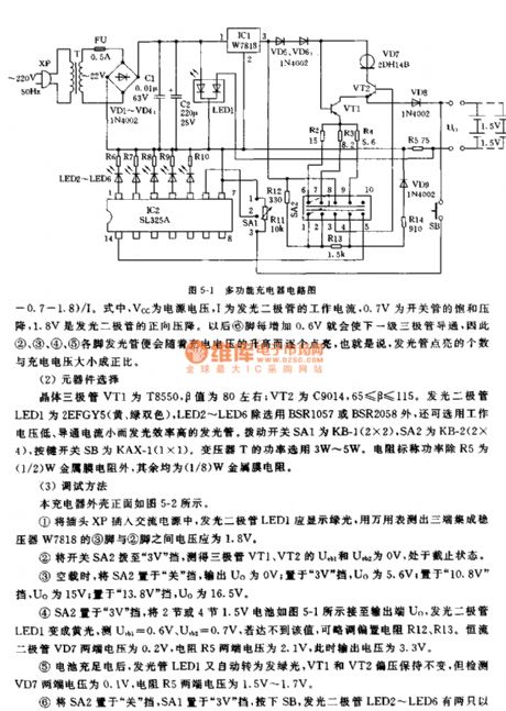
Operating principle:
The circuit is as shown in figure 5-1. You connect the charged battery with the output port Vo, then turn on the power, the transistor VT1 will conduct, the collector electrode of it gets the constant current to charge the battery through the diode VD8. The resistances R12 and R13 are the biasing resistors of the transistor VT2, when the VT2 is in the conduction state, the collector electrode produces the constant collector current because it is connected with the diode VD7, and the constant collector current is output to the collector electrode of transistor VT1 through the emitter, it is used as the load current of VT1 to meet the constant current battery charging. THe VD7 is the constant current diode.
(View)
View full Circuit Diagram | Comments | Reading(672)
VMOS tube switching power supply application circuit (2)
Published:2011/7/13 23:01:00 Author:TaoXi | Keyword: VMOS tube, switching, power supply, application circuit

The VMOS tube switching power supply application circuit is as shown in the figure. Because this circuit uses the voltage comparator 710, the circuit is simplier than former circuits. In this figure, the resistances R1, R2, R3 and the regulator tubes VDl, VD2 form the partial voltage and voltage stabilization circuit, it divides the three groups of voltage (5V, 6V and 18V) from the 28V input voltage to be used as the power of 710; the power soft start-up circuit is composed of the resistances R12, R13, the capacitor C13, the diodes VD6, VD7 and the transistor VT3. In the moment of the power is connecting, the drive pulse width of the VMOS tube VTl increases exponentially.
The rated DC output voltage of this power supply is 5V, the output current is 10A, the operating frequency is 200kHz. (View)
View full Circuit Diagram | Comments | Reading(672)
NE5565 electronic ballast controller
Published:2011/7/13 23:12:00 Author:TaoXi | Keyword: electronic ballast, controller
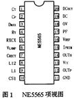
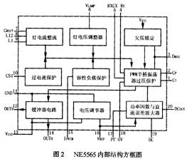
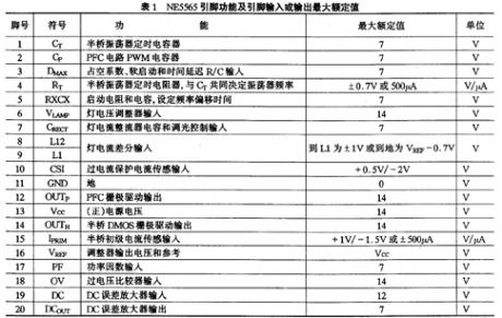
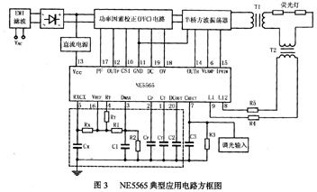
The NE5565 is designed as one kind of electronic ballast controller which is produced by the PHILIPS company. This kind of bipolar type single chip IC integrates the power factor correction (PFC) controller and the self-oscillating half-bridge drive which has the various control and protection functions. By using the NE5565 to design the fluorescent electronic ballast, we can reduce the component number, the volume, the weight and improve the reliability and safety of the ballast.
1. The internal structure and the main features of the NE5565
The NE5565 controller has two switching power supply circuits: the first one is the PFC boost converter controller, it improves the electronic ballast power factor to higher than 0.99, and the current harmonic distortion is extremely low, at the same time it supplies the protection for the AC transient voltage; the second one is the half-bridge oscillator circuit.
(View)
View full Circuit Diagram | Comments | Reading(720)
| Pages:1494/2234 At 2014811482148314841485148614871488148914901491149214931494149514961497149814991500Under 20 |
Circuit Categories
power supply circuit
Amplifier Circuit
Basic Circuit
LED and Light Circuit
Sensor Circuit
Signal Processing
Electrical Equipment Circuit
Control Circuit
Remote Control Circuit
A/D-D/A Converter Circuit
Audio Circuit
Measuring and Test Circuit
Communication Circuit
Computer-Related Circuit
555 Circuit
Automotive Circuit
Repairing Circuit