
Circuit Diagram
Index 1498
μPCl498H field scanning output circuit diagram
Published:2011/7/21 1:34:00 Author:Ecco | Keyword: field scanning output
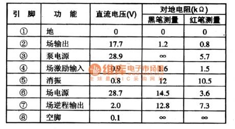
μPCl498H is the new field scanning output integrated circuit produced by Japan NEC, which is widely used in domestic and imported large screen color TV. 1 Features and functionsμPCl498H circuit includes field scanning excitation signal amplifier circuit, field scanning output power amplifier circuit, field scanning pump power supply circuit, vertical blanking pulse generating circuit, and other circuits with auxiliary functions.
(View)
View full Circuit Diagram | Comments | Reading(468)
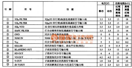
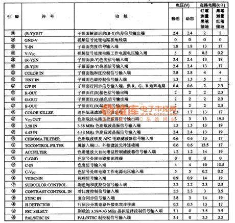
MC141625 - comb filter IC diagram
Published:2011/7/21 1:29:00 Author:Ecco | Keyword: comb filter IC
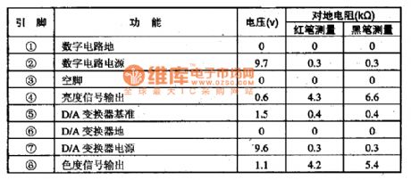
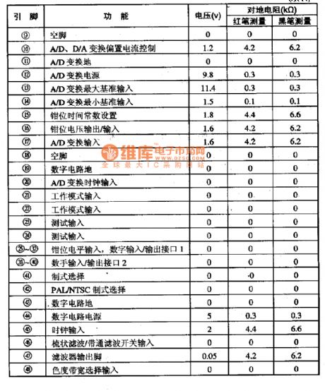
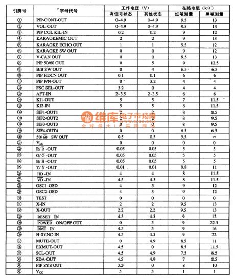
MC141625 is the comb filter integrated circuit manufactured by Motorola, which is widely used in a variety of domestic and imported color television screen, such as Changhong, 2919 series, TDA series, CN-5 movement and so on. MCI41625 IC uses 48-pin dual in-line package, and the integrated circuit pin functions and data are listed in Table. The measured data in the table is from the 2919 series Changhong color TV . In the actual circuit, the MC141625's pin 19 and pin 42 are grounded wires.
(View)
View full Circuit Diagram | Comments | Reading(790)
Automatic gain control amplifier circuit diagram
Published:2011/7/21 1:23:00 Author:Ecco | Keyword: Automatic , gain control amplifier
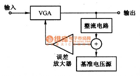
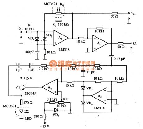
Figure 1 is automatic gain control amplifier. Figure 1 (a) is the block diagram of automatic gain control amplifier which is composed of the variable gain amplifier VGA, rectifier circuit, reference voltage source and error amplifier. Figure 1 (b) is the actual circuit, A1 may constitute VGA amplifier, of which the gain depends on the ratio of resistance value, that is the RG of the optical coupler, and the maximum gain is 15 times which is decided by the ratio of R2 and R1, and the minimum gain is determined by the minimum value of RG.
(View)
View full Circuit Diagram | Comments | Reading(3549)
μPC1830GT PIP integrated circuit diagram
Published:2011/7/21 2:02:00 Author:Ecco | Keyword: PIP integrated circuit
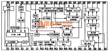
μPC1830GT is the PIP signal demodulation / color demodulation / matrix integrated circuit produced by Japan NEC, which is widely used in domestic and imported large screen color TV. 1. Features and functionsμPC1830GT integrated circuit includes video, chroma, and synchronization processing circuit, and μPC1830GT has PAL and NTSC modem, built-in chroma filter, ribbon-pass filter, luminance delay line and color low-pass filter, and the input signal can be a color video signal or Y / C signal after the separation.
(View)
View full Circuit Diagram | Comments | Reading(1013)
Transistor audio power amplifier circuit diagram
Published:2011/7/21 2:24:00 Author:Ecco | Keyword: Transistor , audio power amplifier
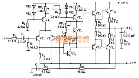
Figure 1 shows the transistor audio amplifier circuit. Flat frequency characteristics of the circuit is 2Hz to 200kHz, and the distortion is below 0.2% at lkHz (30W), and the output power is 30W. VT3 and VT5 form the constant current source circuit, and VT3 collector current is equal to 0.6V / R (RP1), so the resistance of RP1 can be adjusted to change the DC amplifier output bits. VT5 collector current is determined by the 0.6V/R7.
(View)
View full Circuit Diagram | Comments | Reading(6659)
MC145151-2 PLL frequency synthesizer circuit diagram
Published:2011/7/21 2:12:00 Author:Ecco | Keyword: PLL frequency synthesizer
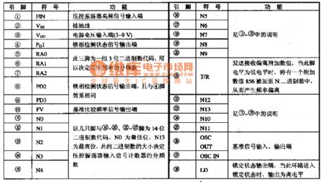
MC145151-2 is the PLL frequency synthesizer IC with dual preset fixed-frequency device. It is suitable for high frequency communications equipment. It has three packages, in order to distinguish by the letter suffix, of which MC145151P-2 is packaged with 28 pin dual in-line package, and MC145151DW-2 is packaged with the 28 pin dual in-line package, and MC145151DW-2 is packaged with the 28-pin package, and MC145151FN-2 is packaged with the SMD ring package. The pin functions are listed in Table.
(View)
View full Circuit Diagram | Comments | Reading(1901)
The Toy tank wireless remote control circuit HS101/HS201
Published:2011/7/18 21:47:00 Author:TaoXi | Keyword: Toy tank, wireless remote control
The toy tank coding emitter circuit:
The toy tank receiving decode circuit:
(View)
View full Circuit Diagram | Comments | Reading(932)
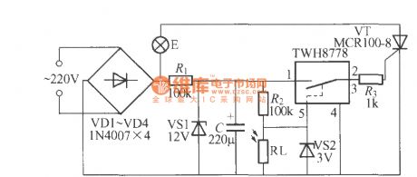
Delay lamp circuit using relay (6)
Published:2011/7/20 2:59:00 Author:zj | Keyword: Delay lamp circuit, using relay
As shown in the figure, delay duration depends mainly on the R and C1 discharge time constant. The magnification of transistor VT1 and VT2affects delay time. The beta is big, the delay time is relatively long. When VT1, VT2 beta ≥100, using data as shown in the figure, the lamp E can be lighted for about 10min each time pressing the switch. (View)
View full Circuit Diagram | Comments | Reading(746)
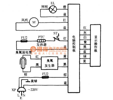
Xintai ZDP-78B computer-controlled horizontal electronic alexipharmic ark circuit diagram
Published:2011/5/13 1:03:00 Author:Ecco | Keyword: Xintai, computer-controlled , horizontal , electronic alexipharmic ark
View full Circuit Diagram | Comments | Reading(623)
Voltage follower circuit diagram
Published:2011/7/20 20:11:00 Author:Ecco | Keyword: Voltage follower
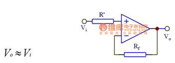
High output resistance and small input resistance can truly transmit input signal to the load, then the signal source currentis low. Voltage follower is a common collector circuit, and the signal is input from the base and output from the emitter, so it is also known as emitter device. Base voltage and collector voltage have the same phase, that is, the input voltage and output voltage is in-phase. The main features of this circuit are: high input resistance, low output resistance, voltage gain is approximately 1, so it is called a voltage follower.
(View)
View full Circuit Diagram | Comments | Reading(791)
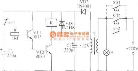
Delay lamp circuit using relay (4)
Published:2011/7/20 3:01:00 Author:zj | Keyword: Delay lamp circuit, using relay
In the graph, K can adopt JZC-22F, DC12V miniature electromagnetic relay. The coil resistance is 400, and contact capacity is 5A. VT1, VT2 require using type 9013 transistor whose performance should be as consistent as possible. Beta value is about 100. Note: VT1 beta value cannot be greater than VT2, otherwise the circuit can not work normally. (View)
View full Circuit Diagram | Comments | Reading(1166)
Benz fault code reading and clearing circuit diagram
Published:2011/7/20 20:18:00 Author:Ecco | Keyword: Benz , fault code , reading , clearing
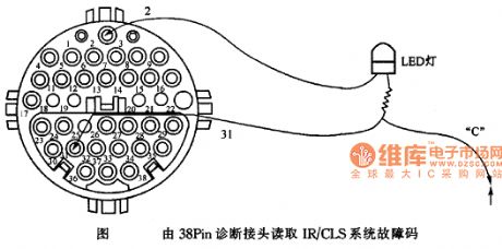
In the figure, the LED light is connected across thesecond and 31th hole ofthe 38th diagnostic connector. (View)
View full Circuit Diagram | Comments | Reading(510)
The typical application circuit and internal block diagram of LAG668B IC
Published:2011/6/23 2:46:00 Author:Ecco | Keyword: typical application, internal , block diagram , IC
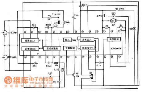
Features of functionLAG668B IC contains two high fidelity pre-amplifier and power amplifier within subwoofer excitation circuit and motor circuit with steady speed. The IC is not combined input capacitor and output coupled capacitor. The block diagram of the circuit and typical application circuit is shown as the circuit. Main electrical parameters The main parameters of LAG668B IC are following:Supply voltage range: 2.3 -4 · 5V, the typical operating voltage is 3V, limit 1 is used as the voltage with 7V.Static current: it is about 18nA. Dynamic operating current: the maximum is 400mA. Because of its large internal resistance, low current, you can get a wide dynamic range both in the case of low and high volume, and the sound quality is good. Power: flat package type is 450mW; dual in-line is 750mW.
The typical application circuit and internal block diagram of LAG668B IC is shown as the chart. (View)
View full Circuit Diagram | Comments | Reading(1029)
Touch type delay lamp circuit using music IC(CIC8251)
Published:2011/7/20 3:03:00 Author:zj | Keyword: Touch type, delay lamp circuit
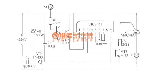
As the diagram shows it is a touch type delay lamp circuit using music IC(CIC8251). It makes use of a music integrated circuit memory function to realize the control delay. The delay time is 1min. The circuit can use common KD-9300serie music IC. But generally this serie music IC are without external oscillation resistance. The circuit delay time is about 20s fixed by chip circuit. (View)
View full Circuit Diagram | Comments | Reading(1243)
TMP87PM36N-R065 single-chip microcomputer integrated circuit diagram
Published:2011/6/23 2:48:00 Author:Ecco | Keyword: single-chip , microcomputer , integrated circuit
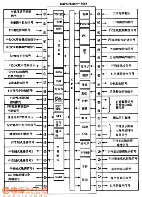
TMP87PM36N-R065 is a single-chip microcomputer integrated circuit produced by Toshiba company, it is widely used in Haier, Toshiba, and other large-screen color TV applications.
1. Features of function
TMP87PM36N-R065 is mainly composed of the central processing unit (CPU), clock oscillator circuit, the reset control circuit, remote command signal processing circuit, the key bits command signal decoding circuit, I2C bus control circuit, audio format control circuit, the screen display characters signal generation and processing circuit, and other control and ancillary functions circuits, the internal circuit block diagram is shown as the chart.
The circuit block diagram and pin functions and signal flowing of TMP87PM36N-R065 integrated circuit 2. Pin functions and data TMP87PM36N-R065 uses 42-pin dual in IC-style package, the pin functions and signal flowing is shown as Figure, the pin letters code and data are listed in Table. TMP87PM36N-R065 IC pin letter code and data
(View)
View full Circuit Diagram | Comments | Reading(784)
TL163 fan ultrasonic remote control integrated circuit diagram
Published:2011/7/20 20:14:00 Author:Ecco | Keyword: fan , ultrasonic , remote control , integrated circuit
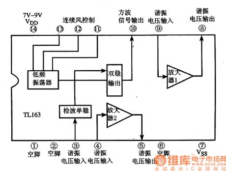
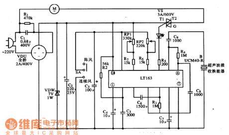
TL163 is a dedicated fan ultrasonic remote control integrated circuit, it is widely used in various high-end remote fan program control circuit. 1. Features TL163 integrated circuit includes two high-gain amplifier, detector, monostable trigger, low-frequency oscillator and bistable drive circuit. The block diagram of the circuit is shown in Figure 1. Figure 1 shows the circuit block diagram and pin functions of TL163 integrated circuit.
2. Pin function TL163 IC uses 14-pin dual in-line plastic package, the pin functions are shown in Figure 1. 3. A typical application circuit The ultrasonic remote control system typical application circuit composed of TL163 integrated circuit is shown in Figure 2. Figure 2 is TL163 IC's typical application circuit
(View)
View full Circuit Diagram | Comments | Reading(2031)
Light control street lamp circuit using MAX837
Published:2011/7/20 3:02:00 Author:zj | Keyword: Light control, street lamp circuit
View full Circuit Diagram | Comments | Reading(740)
Four times pressure fluorescent lamp starting circuit diagram
Published:2011/7/20 20:13:00 Author:Ecco | Keyword: Four times , pressure, fluorescent lamp, starting
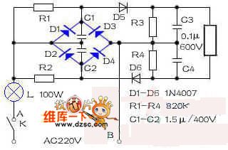
When the A end is positive, B end is negative, the current path is A → L → C2 → D4 → B to make C2 be charged to the peak of electric supply. When the B end is positive, A end is negative, the current path is B → D3 → C1 → L → A to make C1 be charged to the peak of electric supply. At the same time, when A is positive, B is negative, electric supply connected to the voltage on C1 in series will pass D5 to make C3 charge to twice of the peak value; when B is positive, A is negative, electric supply connected to the voltage on C2 in series will pass D6 to make C4 charge to twice of the peak value.
(View)
View full Circuit Diagram | Comments | Reading(638)
The working principle circuit diagram of HT9170
Published:2011/7/20 20:13:00 Author:Ecco | Keyword: working principle
HT9170 will send DTMF signal to the pre-filter (actually a band stop filter) after passing the operational amplifier to filter the 350 ~ 400Hz low frequency interference and noise in DTMF signals. Basically, the output signal contains only two frequencies. The output signals will output high-frequency and low-frequency sine wave signals after respectively passing the two band-pass filters with high-frequency and low-frequency filters, then they will be turned into the rectangular pulses with the same frequency after shaping by the Schmitt circuit.
(View)
View full Circuit Diagram | Comments | Reading(1631)
Battery-powered fluorescent lamp circuit (2)
Published:2011/7/20 20:12:00 Author:Ecco | Keyword: Battery-powered, fluorescent lamp
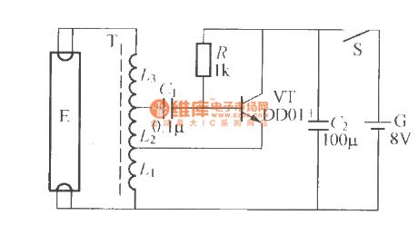
The circuit shown as the chart uses a battery with 8V battery to light 6 ~ 8W fluorescent tube, which can be used in emergency lighting as sudden power outage or flowing palces outdoors . T needs to be made by yourself: it uses E5 ferrite core with Φ0.53 high-intensity polyester, and L1 has 22 turns and L2 has 17 turns around, and L3 switch to uses Φ0.21mm high-intensity polyester enameled wire with 225 turns around, and the head and tail are connected.
(View)
View full Circuit Diagram | Comments | Reading(3001)
| Pages:1498/2234 At 2014811482148314841485148614871488148914901491149214931494149514961497149814991500Under 20 |
Circuit Categories
power supply circuit
Amplifier Circuit
Basic Circuit
LED and Light Circuit
Sensor Circuit
Signal Processing
Electrical Equipment Circuit
Control Circuit
Remote Control Circuit
A/D-D/A Converter Circuit
Audio Circuit
Measuring and Test Circuit
Communication Circuit
Computer-Related Circuit
555 Circuit
Automotive Circuit
Repairing Circuit