
Circuit Diagram
Index 1590
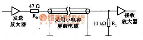
Unbalanced transmission mode circuit diagram
Published:2011/6/26 13:17:00 Author:Sophia | Keyword: Unbalanced transmission mode
(View)
View full Circuit Diagram | Comments | Reading(796)
Timing Controller (the 6th)
Published:2011/7/7 22:34:00 Author:Felicity | Keyword: Timing Controller (the 6th)
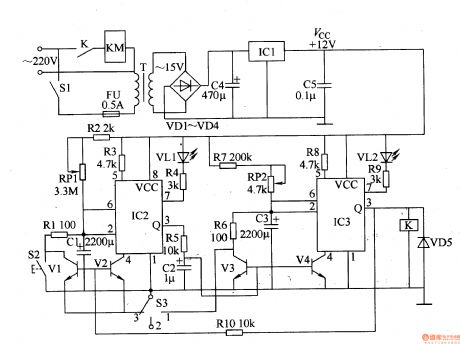
Work of the circuit
The circuit consists of power circuit, timing control circuit and control implementation circuit. (It is showed in picture 8-95.)
Power circuit consists of power switch Sl, fuse FU, power transformer T, rectifier diode VDl-VD4, filter capacitor C4, C5, and three-terminal regulator IC lCl.
Timing control circuit consists of time-base integrated circuit IC2, 1C3, resistors Rl-RlO, capacitors Cl-C3, potentiometer RPl, RP2, transistor Vl-V4, LED VL1, VL2, manual discharge button function selector switch S2 and S3.
Control implementation circuit consists of diode VD5, relay K and AC contactor KM. (View)
View full Circuit Diagram | Comments | Reading(731)
Engine Water Supply Alarm Two
Published:2011/7/7 3:21:00 Author:Felicity | Keyword: Engine Water Supply Alarm
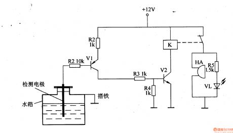
While the water level of the tank is higher than the lowest water level, the water level detect electrode is connected to ground through the resistance of water. V1 is on because of low level voltage of the base, and the high level voltage output by collector is divide by R3 ,R4 and then connect to the base of V2 to make V2 saturated and on and then K is on and the normally off contact of K is off ,then HA is noiseless and VL is off.While the water level in the tank is lower than the lowest water level , the water level detect electrode is above water to make V1 and V2 cut off, and K releases, HA is on and send out alarm, HL is on to warn the driver that the water level of tank is too low and should refill it
(View)
View full Circuit Diagram | Comments | Reading(1768)
Timing Controller (the 5th)
Published:2011/7/7 22:33:00 Author:Felicity | Keyword: Timing Controller
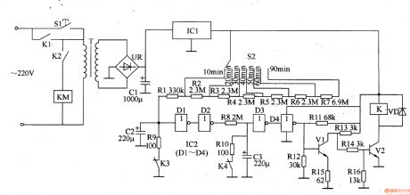
Work of the circuit
The circuit consists of power regulator circuit, timing time circuit, delay circuit and Schmitt trigger control circuit. (It is showed in picture 8-94.)
Power regulator circuit consists of start button SI, power transformer T, bridge rectifier, UR, filter capacitors Cl and three-terminal voltage regulator integrated circuit ICl.
Timing time circuit consists of selector switch S2 and resistors Rl-R7.
Delay circuit consists of capacitors C2, C3, resistors R9, RlO, the normally closed contact relay K K3, K4 and non-gate integrated circuits IC2 (D1-D4).
Schmitt trigger control circuit consists of transistor Vl, V2, resistors RI-R16 and diode VD. (View)
View full Circuit Diagram | Comments | Reading(686)
Engine Water Supply Alarm One
Published:2011/7/7 3:07:00 Author:Felicity | Keyword: Engine Water Supply Alarm
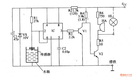
While the engine is not short of water, the electrode of the sensor is connected to ground (the iron) to make the voltage of pin 2 and pin 6 at low level (lower than Vcc/3). The output of pin 3 is at high level to make V1 on, and V2 cut off, then HA is noiseless and HL is off. While the water level of the engine is below the electrode of the sensor, the voltage of pin 2 and pin 6 are at high level (higher than 2Vcc/3). The circuit of IC changes and pin 3 outputs low voltage to make V1 cut off ,and V2 on, and then HA send out beeps and HL is also on to warn the driver the engine is short of water.
(View)
View full Circuit Diagram | Comments | Reading(921)
Beijing City Hunter off-road vehicle non-contact ignition system and charging system circuit diagram
Published:2011/6/30 11:35:00 Author:Sophia | Keyword: Beijing City Hunter off-road vehicle, non-contact ignition system, charging system
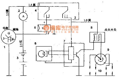
Non-contact ignition system (see Figure 1)
Non-contact ignition system BJ2020SG SUV circuit wiring diagram is shown in Figure 1. In addition to the ignition system suits, the rest of the circuit is unchanged. Non-contact ignition system circuit is shown in Figure 1. Rotor with four poles (with the same number of cylinders) and the stator winding signal generator coil, when the distributor shaft rotates, Non-contact ignition system produces the ignition signal four times a week, the signal voltage input to the ignition module 7. The electronic circuit is used to control turn on and off of the final stage switch tube, when the magnetic-electric ignition signal generator signal is not sent; the ignition coil primary current can flow through the last stage switch tube. When the ignition signal arrives, the last stage switch tube is cut-off, and turn off the primary current, so that the secondary coil generate high voltage, spark plug ignites. (View)
View full Circuit Diagram | Comments | Reading(771)
Timing Controller (the 4th)
Published:2011/7/7 22:31:00 Author:Felicity | Keyword: Timing Controller
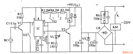
Work of the circuit
The circuit consists of power circuit, the input control circuit, timing circuit and output control circuit. (It is showed in picture 8-93.)
Power circuit consists of Buck capacitor C6, discharge resistors R6, bridge rectifier, UR, filtering capacitor C5, C4 and Zener VS.
The input control circuit consists of the piezoelectric ceramic BC on Electronic alarm clock, capacitor Cl, resistors Rl and transistor Vl.
Timing circuit consists of Resistors Rl-R5, reset button, Sl, regular timing switch S2, capacitor C2 and C3, light-emitting diode VL and time -based integrated circuit IC.
Output control circuit consists of transistor V2, the relay K, the diode VD and AC contactor KM. (View)
View full Circuit Diagram | Comments | Reading(700)
The package and internal structure circuit diagram of integrated chip S-8054ALR
Published:2011/7/7 5:58:00 Author:Sophia | Keyword: package, internal structure, integrated chip S-8054ALR
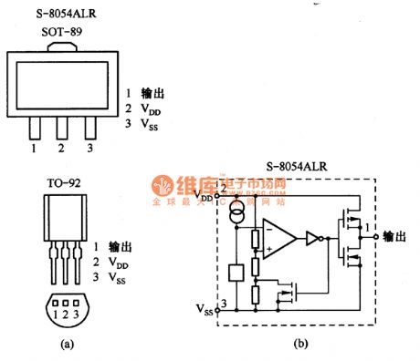
In order to obtain reliable reset signal, dedicated reset IC chips should be adopted. For example, integrated chip S-8054ALR, the package and the internal structure are showed as figure a and b, there are voltage reference and comparator inside the chip to make a comparision between UDD and the reference voltage (S-8054ALR integrated chip of the 4.3 ~ 4.6V) to output signal. (View)
View full Circuit Diagram | Comments | Reading(1562)
The output protection circuit of digital integrated circuit
Published:2011/7/7 6:48:00 Author:Sophia | Keyword: Digital integrated circuit, Output protection circuit
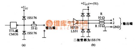
The output of digital integrated circuits must also be protected. Figure a, bare the output protection circuit. Figure a is common protection circuit, Figure (b) is the protection circuit of ELA-422-A. It is the same as the input protection circuit, and resistance R is used to limit the current flowing through output, the diode is used to limit the external input signal level and limit the signal in the range of (0.6V) ~ (Ucc +0.6 V). The resistivity of resistance R is slightly lower than the resistivity of input protective resistance, so that the impact of pressure drop on R can be reduced. (View)
View full Circuit Diagram | Comments | Reading(1585)
Timing Controller (the 3rd)
Published:2011/7/7 22:30:00 Author:Felicity | Keyword: Timing Controller
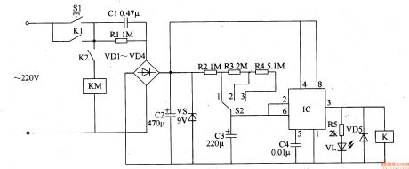
Work of the circuit
The circuit consists of power circuit and timing control circuit. (It is showed in picture 8-92.)
Power circuit consists of Power control button Sl, the normally open relay contact K Kl, step-down capacitor Cl, discharge resistors Rl, rectifier diode VDl-VD4, filter capacitor C2 and Zener VS.
Timing control circuit consists of Time-base IC lC, delay selector switch S2, resistors R2-R5, capacitor C3, C4, light-emitting diode VL, relay K and diode VD5. (View)
View full Circuit Diagram | Comments | Reading(791)
RC reset circuit diagram
Published:2011/7/7 6:19:00 Author:Sophia | Keyword: RC, reset circuit
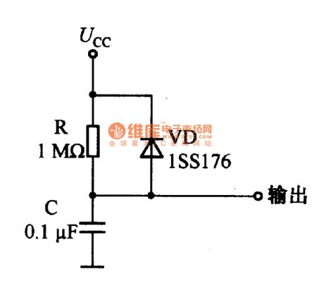
(View)
View full Circuit Diagram | Comments | Reading(3021)
The protection circuit adopting photo-coupler
Published:2011/7/7 7:04:00 Author:Sophia | Keyword: protection circuit, photo-coupler
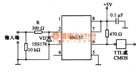
(View)
View full Circuit Diagram | Comments | Reading(962)
The input and output protection circuit of digital integreted circuit
Published:2011/7/7 7:32:00 Author:Sophia | Keyword: Input and output, protection circuit, digital integreted circuit
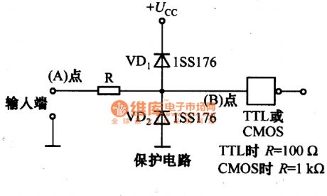
Signal low level UIL of TTL circuit is less than or equal to 0.8V, high UIH is great than or equal to 2.0v. If external digital signal level it receives is within this range, there will be no proplem. In the actual circuit, due to various reasons, the input signal level will be high. Therefore, the input of the digital circuit should be protected from the circuit damaged. Figure is the most common protection circuit. In this circuit, the resistor R is the current limiting resistor, and diode VD1 and VD2 are used to limit the input signal level of digital circuit. The greater R-value, the better the protection, but the voltage drop on input current will be greater. Therefore. For TTL circuits, R should be 100Ω; for CMOS circuits, R is 1kΩ,which will be more appropriate.
(View)
View full Circuit Diagram | Comments | Reading(1848)
The inductance controlled switch circuit (5)
Published:2011/7/2 22:48:00 Author:Borg | Keyword: inductance controlled, switch circuit
This is to introduce an inductance controlled switch circuit which is produced according to the Doppler effect, the circuit is effective when people is within 5m away from it. This circuit can be used in homes, factories, schools and other public spots as the corridor light control or the burglarproof alarm control. The inductance controlled switch circuit consists of the power supply circuit, the Doppler effect oscillator, voltage amplifier, single steady trigger, photo control circuit and control executing circuit and so on, see as the figure. By adjusting R2, the sensibility of the switch can be changed. (View)
View full Circuit Diagram | Comments | Reading(523)
The practical door control burglarproof alarm circuit
Published:2011/7/4 21:58:00 Author:Borg | Keyword: door control, burglarproof alarm
The principle circuit of the device is shown in the figure, which consists of the trigger device, single steady time delay circuit, alarm sound generator, audio power supply circuit, light control circuit, preset lock circuit and power supply circuit, etc. When the room door is shut, the permanent ZT and normally closed reed switch are close to each other, the magnet power of ZT leads to the separation of the 2 contacting chip in AG, so the 6-pin of IC1A is in a high LEV, IC1A is reset, the 5-pin of the output terminal is in a low LEV, the dual-way SCR is blocked without trigger current. (View)
View full Circuit Diagram | Comments | Reading(658)
Proximity Switch Circuit Composed Of Integrated Magnetic Sensor HMC1001
Published:2011/7/7 6:52:00 Author:Robert | Keyword: Proximity, Switch, Integrated, Magnetic Sensor
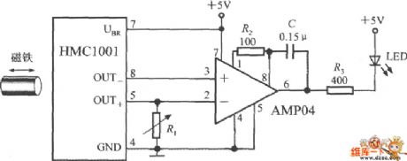
The picture shows the proximity switch circuit composed of the HMC1001 and operational amplifier (AMP04) and light emitting diode (LED). The operational amplifier is used as a comparator here. If taking a magnet with length about 6mm~12mm to close to the HMC1001, when it moves to a certain position, the MR electric bridge's output voltage would be 30mV to flip the comparator and then it outputs low voltage level to make LED light. If remove the magnet the comparator would output high voltage level to stop LED lighting. Obviously, the circuit is equivalent to the proximity switch with indicating light. It can be used for detecting displacement, rotating speed and other non-electricity parameter. By adjusting R1's resistance value it can set the switch's threshold voltage. (View)
View full Circuit Diagram | Comments | Reading(2932)
555 Time-Base Circuit Main Parameters Circuit
Published:2011/7/7 8:19:00 Author:Robert | Keyword: Time-Base, Main, Parameters
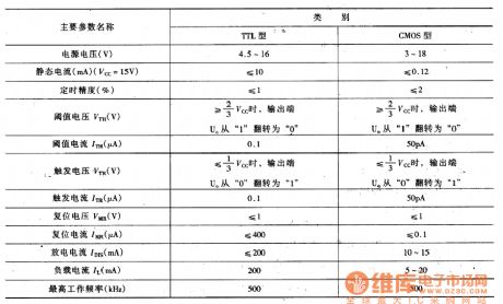
For correctly using the 555 time-base circuit, we should know about its main parameters. The TTL type and CMOS type 555 time-base circuits have difference in their features and parameters. So this table listed their main parameters separately to be used for reference. For dual time-base circuit, the parameters are all the same with the single time-base circuit's except for the its doubling quiescent current. So it can be used by taking the single time-base circuit's main parameters as the reference.
The table shows the 555 time-base circuit's main features and parameters. (View)
View full Circuit Diagram | Comments | Reading(1087)
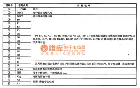
CW6510 Electronic Musical Instruments Single-Chip Micro-Computer Integrated Circuit
Published:2011/7/7 6:19:00 Author:Robert | Keyword: Electronic, Musical Instruments, Single-Chip, Micro-Computer, Integrated
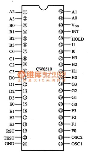
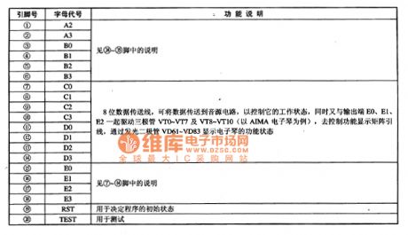
The CW6510 is a special electronic musical instruments single-chip NMOS four-bit micro-computer (CPU) IC produced by the Japanese Sanyo company. It is widely used in many brands of electronic organ.
1.Its functional features.
The CW6510 IC's internal part is made up of clock oscillation circuit, reset control circuit, testing circuit, key-bit matrix circuit, scanning pulses generating circuit, key command signal coding circuit, data signal input/output interface circuit, interrupt request control circuit. Its internal part has been installed the special programs of scale generating and sound simulation, percussion music, rhythm, tutti and so on.
2.Its pin's function.
The CW6510 IC uses 42-pin dual inline package. Its shape is shown in picture 1 and its pin's function is listed in table 1. This IC's power voltage's typical value is 5V (4-6V is also OK). Its rated output current is ±2mA (for every function output port). (View)
View full Circuit Diagram | Comments | Reading(1268)
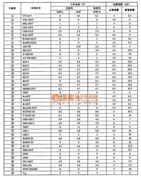
CTV225S-PRC1 Single-Chip Micro-Computer Integrated Circuit
Published:2011/7/7 6:29:00 Author:Robert | Keyword: Single-Chip, Micro-Computer, Integrated
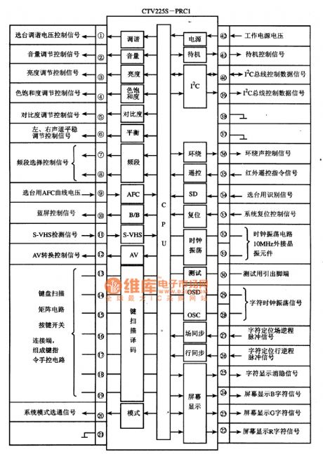
The CTV225S-PRC1 is a single-chip micro-computer IC which is widely used in sony, hitachi etc. series digital color TV sets' system control circuits.
1.Its functional features.
The CTV225S-PRC1 IC's internal part is mainly made up of central processing unit (CPU), clock oscillation circuit, reset control circuit, key scanning coding and decoding circuit, I2C bus control circuit, remote-control command signal processing circuit, screen display character generating and processing circuit, standby and starting power control circuit, system mode selection circuit, and other some control and auxiliary function circuit.
2.Its pin's function and data.
The CTV225S IC uses 42-pin dual inline package. Its pin's function and signal flowing is shown in picture 1 and its pin's letter code and data is listed in table 1. Its internal circuit diagram and pin's function and signal flowing is shown in picture 1. (View)
View full Circuit Diagram | Comments | Reading(747)
The single-way SCR simple touching switch circuit
Published:2011/7/8 0:43:00 Author:Seven | Keyword: single-way SCR, touching switch
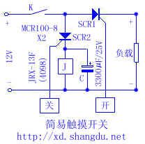
In the experiments, the writer found that the control pole of single-way MCR100-8 is conducting with a hand touch without the forward voltage, therefore, the writer designed a simple touching switch, see as the figure.
By one touch, the metal chip is open, SCR1 is conducting, and the load is getting power. And with another touch, the metal plate is closed, SCR2 is conducting, relay J is getting power and working, K is cut off, the load loses effect. After SCR is cut off, the capacitor discharges to relay J, which keeps the relay closed for 4 seconds or so. (View)
View full Circuit Diagram | Comments | Reading(1565)
| Pages:1590/2234 At 2015811582158315841585158615871588158915901591159215931594159515961597159815991600Under 20 |
Circuit Categories
power supply circuit
Amplifier Circuit
Basic Circuit
LED and Light Circuit
Sensor Circuit
Signal Processing
Electrical Equipment Circuit
Control Circuit
Remote Control Circuit
A/D-D/A Converter Circuit
Audio Circuit
Measuring and Test Circuit
Communication Circuit
Computer-Related Circuit
555 Circuit
Automotive Circuit
Repairing Circuit