
Circuit Diagram
Index 1592
Illumination Controller (8)
Published:2011/7/6 5:41:00 Author:Sue | Keyword: Illumination, Controller
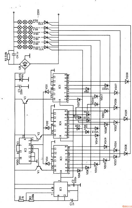
The 220v ac voltage will provide IC1,IC2 and V1-V3 with 9V working voltage after it is reduced by C4, rectificated by UR, stablized by VS, filtrated by C.
After IC2 is connected and reset, its Y0 terminal(pin 3) will output high level which will make V1 connected. IC3 will be connected and begins to work. At the same time, the oscillator also begins to work. Then IC1's pin 3 will output oscillate signals which will serve as the count pulse of IC3-IC5.
After IC3 begins to count, its Y1 terminal will output high level. VD4 is connected which will make VT1 connected. The first circuit of illuminations HL1 will be illuminated.
When IC3's Y2 terminal outputs high level, Y1 terminal returns to low level. VD8 is connected which will make VT2 connected. The second circuit of illuminations HL2 are illuminated while HL1 are off. (View)
View full Circuit Diagram | Comments | Reading(611)
Illumination Controller (7)
Published:2011/7/6 0:26:00 Author:Sue | Keyword: Illumination, Controller
The 220v ac voltage will generate 9V voltage after it is rectificated by VD13-VD16, reduced by R3, stablized by VS, filtrated by C3. The voltage will provide IC1 and IC2 with working voltage.
After the multivibrator begins to work, IC1's pin 3 will output oscillate signals which will serve as IC2's count pulse. Then IC2 begins to count and Y0-Y9 will output high level in turn.
When IC2's Y0 terminal(pin 3) outputs high level, its high level will be put on VT1's gate electrode through VD1 which will make VT1 connected. The first circuit of illuminations HL1 are illuminated.
When Y1 terminal outputs high level, Y0 terminal has low level again. VD2 is connected which will make VT2 connected. The second circuit of illuminations HU are illuminatedwhile HL1 are off. (View)
View full Circuit Diagram | Comments | Reading(608)
Illumination Controller (6)
Published:2011/7/6 0:20:00 Author:Sue | Keyword: Illumination, Controller
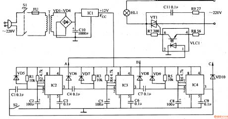
When the power switch S1 is connected, the 220v ac voltage will provide the univibrator circuit with working voltage afterit is reduced by T, rectificated by VD1-VD4, filtrated by C10, stablized by IC1.
S2 is the trigger switch. When S2 is pushed, IC2's pin 2 will output a negative pulse,which will make the univibrator composed of IC2 reverse. IC2's pin 3 will output high level, which will make the optical coupler VLC1's inner LED illuminated. The optical transistor is connected which will make bidirectional triode thyristor VT1 connected. The first group of illuminations HL1are illuminated. (View)
View full Circuit Diagram | Comments | Reading(656)
Illumination Controller (5)
Published:2011/7/6 0:10:00 Author:Sue | Keyword: Illumination, Controller
When the power is on, the 220v ac voltage will generate about 6V direct current voltage after it is reduced by C6,stablized by VS,rectificated by VD, filtrated by C5. The voltage will provide IC1 and IC2 with working voltage.
When S1 is pushed, IC2's pin 13 will input a high level pulse. IC2 will be altered to the other illumination mode automatically. When IC2's pin 7-10 output high level, the controlled thyristors VT1-VWwill beilluminated. When IC2's pin 7 outputs high level, VT1 is connected and the first circuit of illuminations HL1are illuminated. When IC2's pin 8 outputs high level, Vm is connected and the second circuit of illuminations HL2are illuminated. When IC2's pin 10 outputs high level, VT4 is connected and the 4th circuit of illuminations HL4are illuminated. (View)
View full Circuit Diagram | Comments | Reading(606)
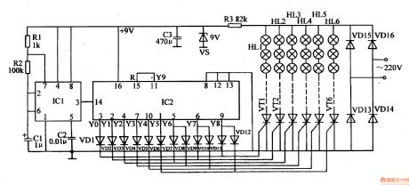
Illumination Controller (10)
Published:2011/7/6 0:43:00 Author:Sue | Keyword: Illumination, Controller
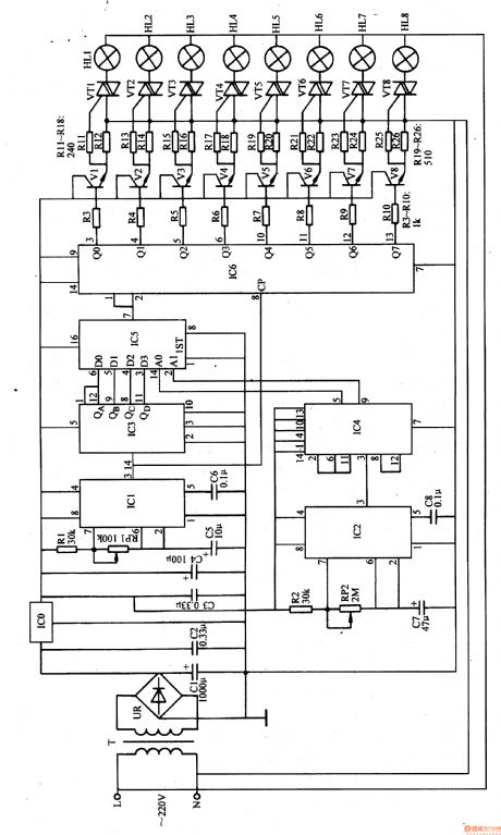
When the power is on, the 220v ac voltage will provide IC1-IC6 with +5v direct current working voltage after it is reduced by T, rectificated by UR, filtrated by C1 and C2, stablized by ICO.
After the multivibrator A begins to work, IC1's pin 3 will output low-frequency oscillate signals. One serves as IC3's count pulse. The other serves as IC6's shift clock pulse.
After IC3 begins to work, the count pulse signals will be counted and frequency-divided. Its pin 12, pin 9, pin 8, pin 11 will output count pulse's 2nd,4th,8th,16th frequency-divided signals respectively. (View)
View full Circuit Diagram | Comments | Reading(605)
Illumination Controller (4)
Published:2011/7/6 0:11:00 Author:Sue | Keyword: Illumination, Controller
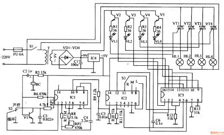
When the power switch S1 is connected, the ac 220v voltage will provide V2-V5 with 9V direct current working voltage after it is reduced by T,rectificated by VD1-VD4, filtrated by C1. The other circuit will provide the voice-operated circuit, oscillator and controller with +5v voltage after it is stablized by rC4. After the oscillator works, IC1's pin10 will outputoscillatepulse signals which will serve as IC2's control pulse. IC3 will output pulse control voltage under the control of IC2. Then the illuminations will be on and off as VT1-VW is connected and disconnected under the control of V2-V5. (View)
View full Circuit Diagram | Comments | Reading(910)
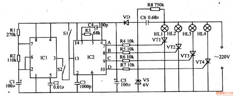
Illumination Controller (11)
Published:2011/7/5 6:29:00 Author:Sue | Keyword: Illumination, Controller
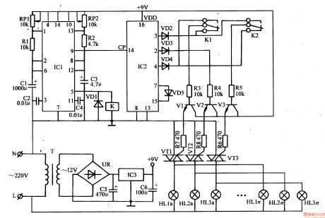
After the clock oscillator begins to work, IC1's pin 9 will output low-frequency oscillate signals as IC2's count pulse. Then IC2 begins to count and Y0-Y3 will output high level one by one which will make V1-V3 and VT1-VT3 connected in turn. Then the 3rd illuminations are illuminated in turn.
The circuit is a low-frequency oscillator. After it begins to work, IC1's pin 5 will output low-frequency pulse signals. When IC1's pin 5 outputs positive pulse, K is connected and K1's,K2's normally open contactors are connected while normally closed contactors are disconnected. When IC1's pin 5 outputs negative pulse, K is released. K1's and K2's nomally closed contactors are connected and nomally open contactors are disconnected. (View)
View full Circuit Diagram | Comments | Reading(562)
Illumination Controller (3)
Published:2011/7/5 23:45:00 Author:Sue | Keyword: Illumination, Controller
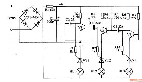
When the working power is on, the thyristor V3 is the first to be connected(because V3's base bias resistance value is lower than V1's and V2's), its collector becomes low level. Because capacitor C4's voltage can't realise abrupt change, and V2's base voltage is close to 0V, V2 is disconnected. V2's collector has high level. The thyristor VT2 is connected and the 2nd circuit of illuminations HL2 are illuminated. V2's collector's high level makes V1 connected through C3. V1's collector has low level and VT1,VT3 are disconnected. The 1st circuit of illuminations HL1 and the 3rd circuit of illuminations HL3 are not illuminated. (View)
View full Circuit Diagram | Comments | Reading(530)
Part of Switching Power Supply Circuit
Published:2011/7/1 2:21:00 Author:Joyce | Keyword: Part , Switching Power Supply
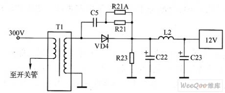
As shown in the figure, the 12 V voltage is not stable, therefore, the output part of the switching power supply should be examined first. Check whether the secondary winding of the switch transformer and VD4 function properly and make sure that inductance L2 has no cold solder joint. Parameters of filter capacitance C22 and C23 are 1000 pF / 16 V.If one uses the capacitance meter to measure C23, one will find that it works properly (capacity declines slightly), but the capacity of C22 drops to less than 80 uF. The reason is that the main source of the machine is installed at the base of the monitor, which is small and has low heat dissipation, while C23 and C22 both are close to the 12 V rectifier diode (especially C22), so their capacity would decline after baking, to lower the loading ability of the voltage, which further leads to this fault.
(View)
View full Circuit Diagram | Comments | Reading(619)
wireless remote control/touch dimmer circuit(RCM1A/RCM1B)
Published:2011/6/20 8:10:00 Author:Lena | Keyword: wireless, remote control, touch dimmer
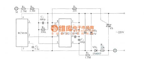
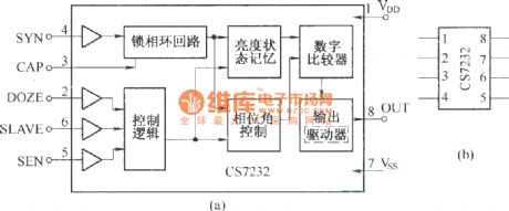
Wireless remote control/touch dimmer circuit is an incandescent lamp dimmer switch with wireless remote control component RCM1A/RCM1B and touch dimmer integrated circuit CS7232 as the core. It can be used to control droplight, reading lamp and wall lamp etc, provided with small bulk, convenient usage, stable and reliable work characteristics.CS7232 is a CMOS type integrated circuit used to control incandescent lamp dimmer. It can control breakover of bidirectional thyristor to realize lamp brightness control, provided with low power loss, multi purpose , high sensitivity etc characteristics.
(View)
View full Circuit Diagram | Comments | Reading(1427)
TMP47C400RN Microwave/Oven Monolithic Micro Computer Control Integrated Circuit Diagram
Published:2011/7/3 1:56:00 Author:Vicky | Keyword: Microwave, Oven , Monolithic Micro Computer Control
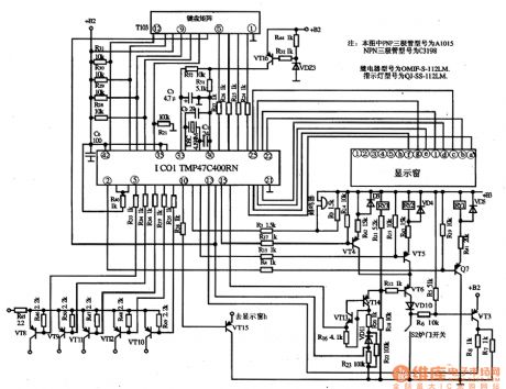
Picture 1 is the typical applied circuit diagram of TMP47C4OORN integrated circuit.
TMP47C400RN is a chip specially designed by Japanese Toshiba Corporation for microwave/oven.
1 functions and features
TMP47C400RN integrated circuit includes keyboard matrix circuit, clock oscillator circuit, motion circuit, reset circuit, microwave control circuit, oven light control circuit and other accessory circuits.
2 pin functions and datum
TMP47C400RN integrated circuit adopts 42 pins in biserial package.
3 typical applied picture
Typical applied circuit of IC TMP47C400RN is shown in the above picture.
Note: When the microwave or oven does not work, you should first check if the 12V AC in the pin 42 of the IC TMP47C4OORN is normal or not, then check the reset signal in the pin 33 (it presents low level at the moment of starting up, and high level during normal work) and the clock oscillating signal pins 31&32.
(View)
View full Circuit Diagram | Comments | Reading(5157)
Circuit Diagram of SL322-Type Flexible and Light-Spot Displaying Level Indicator
Published:2011/7/2 0:04:00 Author:Vicky | Keyword: Flexible and Light-Spot Displaying , Level Indicator
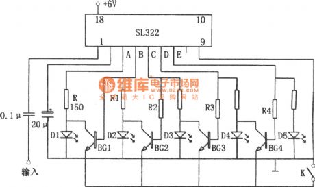
The circuit is made of luminous display driver SL322, luminous diodes from D1 to D5, transistor from BG1 to BG5 etc.
When K is closed, all the triodes’ emitters are in ground connection state. When the level rises to make luminous diode D2 give out light, electrical potential of B rises, BG1 is conducted, and then the luminous diode D3 goes out. When the electrical potential rises to make the D3 luminous, then electrical potential of C rises, BG2 is conducted, and thereby D2 goes out. In the context, due to the unchanged electrical potential of B, BG1 is still off, and D1 is still lightless. Ultimately, when the electrical potential rises to make D5 give out light, transistors form BG1 to BG4 are conducted, and luminous from D1 to D4 all die out, which formulates light-spot displaying. When the switch K is disconnected, all triodes stop working, and the light-spot displaying ends. (View)
View full Circuit Diagram | Comments | Reading(673)
Non-Volatile Memory Integrated Circuit Diagram
Published:2011/7/7 8:37:00 Author:Vicky | Keyword: Non-Volatile, Memory Integrated Circuit
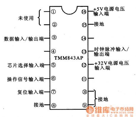
Picture 1: Ranking of IC TMM8432AP pin
TMM843AP is a non-volatile memory integrated circuit produced by Toshiba Corporation. It is widely used in control system of color television , DVD player, audio device, and air-conditioner, mainly for saving information and program.
1 functions and features
Internal part of IC TMM843AP is mainly composed of data storage UO interface circuit, chip selection circuit, reset control circuit, time base circuit, operating signal processing circuit and some other auxiliary functional circuits.
2 function and data of pins
IC TMM8431P uses 16 pins which are in dual-in-line package. The ranking of the pins are as shown in picture 1.
Note: If the memory function does not work, check whether the power supply voltage of + 32V in the pin 12 works regularly or not first. (View)
View full Circuit Diagram | Comments | Reading(945)
Circuit Diagram of Audio Logic Level Probe Composed of 555
Published:2011/7/2 22:11:00 Author:Vicky | Keyword: Audio Logic Level Probe
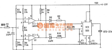
The above picture is audio logic level probe circuit, which is composed of voltage comparator, multivibrator, and piezoelectric ceramics HTD etc. The latter two constitute audio circuit and the audio frequency is used to assess the TTL or COMOS instrument’s electrical level.
When the probe reaches high level, IC-1 sends out signal to make D2 conducted and charge C1 via R9 and R11. The oscillator works, and the correspondent oscillating frequency is fH=1.44/(R10+2R11)C1, the correspondent frequency of the parameter in the picture is abouth 4kHz. When the probe reaches low level, the matched D3 is conducted, and C1 is charged via R10 and R11. The correspondent oscillator circuit works with oscillating frequency of fL=1.44/(R10+2R11)C, and the correspondent frequency of the parameter in the picture is about 700Hz. When pulse train is detected, the correspondent HTD sends out mixed sound or trill sound. (View)
View full Circuit Diagram | Comments | Reading(2113)
LCD Backlight Luminance Auto-control Circuit (Visible Light Luminance Sensor LX1970) Diagram
Published:2011/7/7 8:36:00 Author:Vicky | Keyword: LCD Backlight, Luminance Auto-control Circuit , Visible Light Luminance Sensor
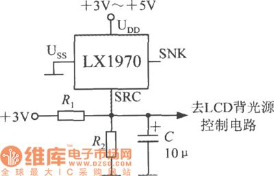
When it turns dark, LX1970 will automatically start up the LDC backlight to make white LED luminous. Luminance auto-control circuit is shown in the picture. The maximum and minimum value of the luminance can be controlled and set by resistances R1 and R2. The responding time and leaching of disturbance of 50Hz power grid can be adjusted by changing the capacity of capacitance C. LX1970 adopts +3.3 to +5V power supply. When only SRC end is used, the SNK end should hang in air. Suppose that the white LED is driven by 0.25~1.25V output voltage, then 0.25V is the minimum luminance value of LED while 1.25 is the maximum value. (View)
View full Circuit Diagram | Comments | Reading(978)
Simple-Adjustment Type High Input Impedance Double-Wave Linear Detection (CR4558DN) Circuit Diagram
Published:2011/7/1 23:57:00 Author:Vicky | Keyword: Simple-Adjustment, High Input Impedance Double-Wave Linear
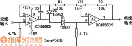
The above picture is a simple-adjustment type high input impedance double-wave linear detection circuit.
In the positive semi-circle of output AC signal, the output of A1 is positive, and forward biased D1 is conducted, and therefore both the input and output of A2 are positive. Use R2, VR1,and R1 to perform reverse feedback of β=1 towards A1, that is to say, to change A to be non-inverting amplifier with gain of 1 . Under such circumstance, the gain remains unchanged when modulate VR1.
In the positive semi-circle of the output signal, the output of A1 is negative, D1 is reverse biased, the output of A2 is 0, and therefore A2 becomes inverting amplifier. A1 conducts reverse feedback via D2. In fact, A1 becomes voltage follower. The reverse output of A2 is identical with AC input voltage, and A2 works as a invert amplifier with gain of 1. Under such circumstance, the gain of A2 can be changed by modulating VR1. Modulate VR1 to ensure that the whole gain is 1. (View)
View full Circuit Diagram | Comments | Reading(679)
Internal Block Circuit Diagram of IC LA445
Published:2011/7/7 8:39:00 Author:Vicky | Keyword: Internal Block Circuit Diagram
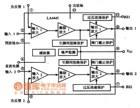
LA445 is a dual-channel audio power amplifier integrated circuit produced by Japanese SANYO Electric. It is widely used in home audio device, vehicle audio device, television audio system, and computer audio System.
Functions and Features
IC LA445 consists of dual-channel audio power amplifier circuit, short-circuit protection circuit, overvoltage protection circuit, surge suppressor circuit, and thermal cutoff circuit. It has various features, such as strong restraining capacity of ripple wave, high separating degree, good balance, and convenient assembling of radiator. It can constitute dual-channel or BTL power amplifier.
The limit working voltage of IC L445 is 25V, maximum quiescent current is 100mA, and typical value is 75mA. Its internal block circuit diagram is shown in the picture. (View)
View full Circuit Diagram | Comments | Reading(1439)
The battery, starter and engine circuit of Passat 2.81V
Published:2011/7/7 21:17:00 Author:Seven | Keyword: engine circuit, starter
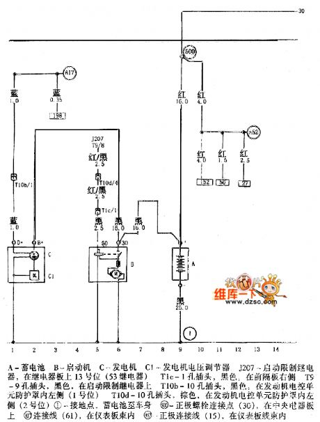
The battery, starter and engine circuit of Passat 2.81V is shown as above.A-battery B-starter C-generator C1-voltage regulator of the generator J207- the starting limit relay, on the 13 spot of the board(53 relay) T1c-one-hole plug, black, on the right side of the angle divider T9-9-hole plug, black, on the starting limit relay T10b-10-hole plug, black, on the left side of the shield of the generator control unit(No.1 spot)T10d-10 -hole plug, black, on the left side of the shield of the generator control unit(No.2 spot)①-ground connection spot, from the battery to the car body (View)
View full Circuit Diagram | Comments | Reading(1151)
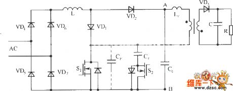
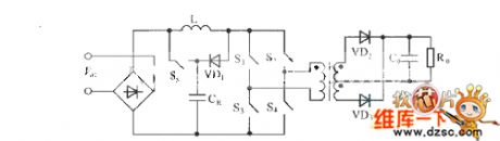
The Booster single-stage separated PFC converter circuit of active clamper and soft switch function
Published:2011/7/7 4:43:00 Author:Seven | Keyword: single-stage, PFC converter, soft switch
View full Circuit Diagram | Comments | Reading(911)
The PFC converter circuit of I3 parallel connected single-stage Boost type
Published:2011/7/7 4:38:00 Author:Seven | Keyword: PFC converter, single-stage
View full Circuit Diagram | Comments | Reading(565)
| Pages:1592/2234 At 2015811582158315841585158615871588158915901591159215931594159515961597159815991600Under 20 |
Circuit Categories
power supply circuit
Amplifier Circuit
Basic Circuit
LED and Light Circuit
Sensor Circuit
Signal Processing
Electrical Equipment Circuit
Control Circuit
Remote Control Circuit
A/D-D/A Converter Circuit
Audio Circuit
Measuring and Test Circuit
Communication Circuit
Computer-Related Circuit
555 Circuit
Automotive Circuit
Repairing Circuit