
Circuit Diagram
Index 1600
Calendar and clock display interface circuit
Published:2011/7/2 0:23:00 Author:Fiona | Keyword: Calendar and clock, display interface
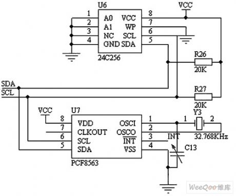
As shown in figure,this display interface is composed of EEPROM24C256 and calendar clock chip PCF8563.24C256 is a low voltage, serial interface and 256K capacity memorizer which is used for storing the measured blood pressure values.PCF8563 is a industrial multi-functional clock/calendar chip containing the I2C bus with very low power consumption which is introduced by PHILIPS company. It used for providing the time and date of blood pressure measurement so that it can be used and inquired afterwards.It is convenient for users to have a clear memory for their period blood pressure.It is practical and overcome the shortage of some electronic sphygmomanometer.
(View)
View full Circuit Diagram | Comments | Reading(1199)
the controller circuit of the fish brood pond part 2
Published:2011/6/13 8:43:00 Author:Ariel Wang | Keyword: controller, fish , brood, pond
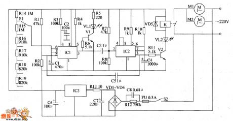
After the power circuit gets through,it provides +12V voltage to the pin-8 of IC1.It provides reset signal for IC1's pin-4 by resistence R3 and capacitor C2(at the moment when the power is on it is low level,then it stays high level ).Then the in-circuit of IC2 is forced to reset.The pin-3 is output low level.It stops V1.And it generates low level trigger pulse at the pin-2 of IC2.It turns the voltage of pin-3 from low level to high level.V2 is conducted.Relay K is pulled in.The open points is conducted. The electric motor of water pump M1 and the electric booster pump M2 are conducted to work.VL2 is lighted.The high level outputs from pin-3 of IC2 gives a feedback to pin-2 of IC1 by capacitor C5.Then IC2 stays reset.
(View)
View full Circuit Diagram | Comments | Reading(547)
The interface circuit of nRF2401 and CY7CS323
Published:2011/7/1 8:08:00 Author:Fiona | Keyword: interface circuit, mode
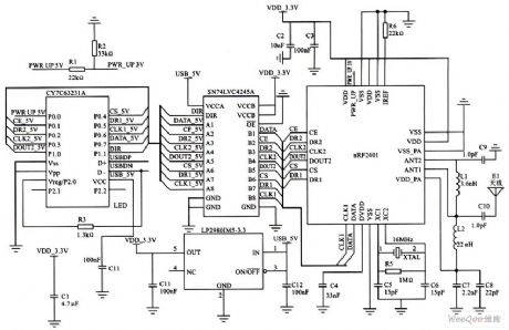
In the figure,CY7C63231 is 8-bit RISC microprocessor,it's especially suitable for the USB embedded side,the working voltage is 5V.nRF2401 is single-chip RF transceiver chip,it has four operating modes:send and receive mode,configuration mode,idle mode and off mode.All configuration,operating mode selection and sending and receiving are all completed through the control of CY7C63231's PO pin.It produces the working voltage (3.3 V) of nRF2401 by using voltage adjustment chip LP2980IM5-3.3,meanwhile,SN74LVC4245 produces 3.3 V control port and 5 V level translation, so that two kinds of chips can normally connect in different voltages.
(View)
View full Circuit Diagram | Comments | Reading(1847)
the circuit of heat alarm for rice seedbed
Published:2011/6/14 7:05:00 Author:Ariel Wang | Keyword: heat, alarm, rice, seedbed
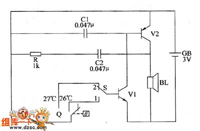
the working principle of circuitWhen the rice seedling has two leaves and one needle,you can put the transfer switch to the position of 2 .At this time,the temperature of the alarm is 27℃.When the temperature of the shed is below 27℃,the oscillator doesn't work.BL doesn't give a sound.When the temperature reaches or goes beyond 27℃,the oscillator works.BL gives the alarm sound.When the rice seedling has three leaves and one needle,you can put S to the position of 1 .When the temperature of the shed is lower than 26℃,BL doesn't give a sound.When it's higher than 26℃,it gives the alarm sound.
(View)
View full Circuit Diagram | Comments | Reading(517)
Interface circuit of LPC2200 and PDIUSBD12
Published:2011/7/1 7:19:00 Author:Fiona | Keyword: Interface circuit
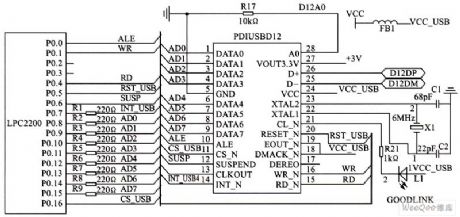
PDIUSBD12 uses the Bank2 part of LPC2200 external memory control,the data address is 0x82000000, the command address is Ox82000001. RST_USB, SUSP are the LPC2200's output pins, PDIUSBD) 12 interrupt signal is the interrupt input signal and an external interrupt O. C1, C2 and X1 offer PDIUSBD) 12 the clock input for the work.LED GoodLink flickers during normal communication.The AD0 of PDIUSBD12 is connected to the A0 of LPC2200,when the LPC2200 outputs 1 through the A0 pin, it shows that the data which outputs to the PDIUSBD12 data bus DO ~ D7 is command word; When the A0 pin outputs 0,it shows that the data which outputs to the PDIUSBD12 data bus DO ~ D7 is data word.
(View)
View full Circuit Diagram | Comments | Reading(1134)
the controller circuit of fish incubation pool part 1
Published:2011/6/15 7:47:00 Author:Ariel Wang | Keyword: controller, fish , incubation, pool
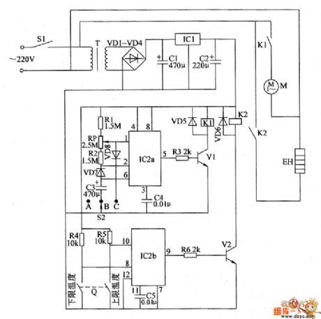
When S2 is put at the position of “A”, pin-2(threshold end) and pin-6(low-triggering end) of IC2 output high level.Pin-5 outputs low level.It stops driving transistors V1.Relay K1 doesn’t pull in. The oxygen pump stops working. When S2 is put at the position of “C”,pin-2 and pin-6 of IC2 output low level.Pin-5 outputs high level.V1 is conducted..K1 contacts pull in.The oxygen pump is conducted to work.. It continues to pump oxygen into the fish pool.When S2 is put at the position of “B”,IC2a is working with the interval oscillator.It outputs rectangular impulse from pin-5.It conducts V1 at an interval time.The oxygen works at an interval time.It pumps right amount of oxygen into the fish pool.
(View)
View full Circuit Diagram | Comments | Reading(538)
Circuit Diagram of Gaining 0~433V voltage by star connection of three voltage regulators
Published:2011/6/25 10:47:00 Author:Vicky | Keyword: 0~433V voltage, star connection of three voltage regulators
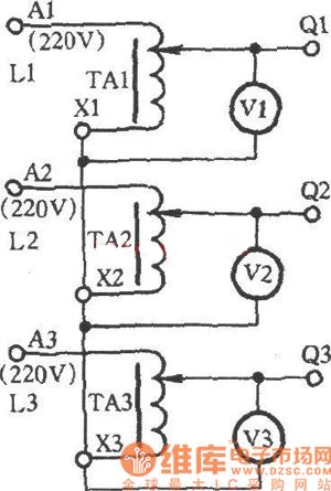
As shown in the picture, by adopting star connection of three voltage regulator (TA1, TA2, and TA3), the range of voltage regulating is expanded and the highest voltage can be 433V. Connect X1, X2 and X3 together which belong to TA1, TA2 and TA3 respectively, and connect A1, A2, and A3 triphase L1, L2 and L3 of 380V power supply, so that 433V voltage is gained in the output end of Q1 and Q2 or Q2 or Q3. However, this connection methond requires balance of triphase voltage, and the type and specification of TA1, TA2, and TA3 should also be the same. (View)
View full Circuit Diagram | Comments | Reading(710)
Voltage Regulator Voltage and Load Test Circuit Diagram
Published:2011/6/25 10:43:00 Author:Vicky | Keyword: Voltage Regulator Voltage and Load Test
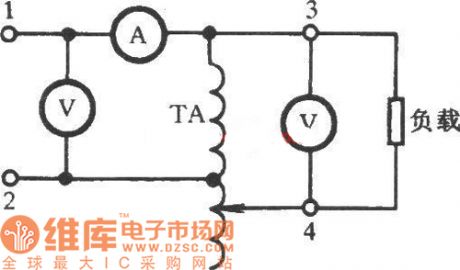
Voltage regulator voltage and load test is shown as in the picture. Make the AC input ends1 &2 of the voltage regulator connected to standard voltage of 220V; make the secondary ends 3 & 4 connected to AC voltmeter V; spin the voltage regulator hand wheel and then the secondary output voltage should rise to 250V from 0V. In processing load test, ends 1 & 2 are connected to standard voltage of 220V, and secondary 3 & 4 are connected to the load. For example, a voltage regulator of 1KVA can be connected to electric stove of 1KW and concatenated with AC voltmeter A. Spin the voltage regulator hand wheel , and then the current reaches rated current value of 4A and keep the power on for 2 hours. If no abnormal phenomena such as smoking and smell of burning arise, the quality of voltage regulator TA is good. (View)
View full Circuit Diagram | Comments | Reading(864)
The traditional RS485 interface circuit
Published:2011/7/1 22:57:00 Author:Fiona | Keyword: traditional RS485 interface
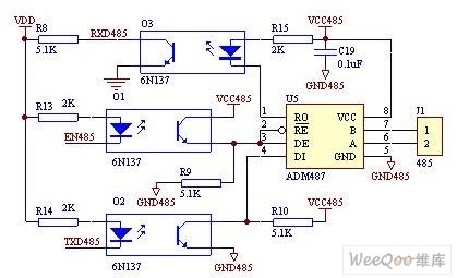
Used as a common communications interface devices, RS-485 / RS-422 chip can find corresponding models in many semiconductor companies, such as the ADI company ( device prefix is ADM).Most of the industrial RS-485 bus's customers should use the following circuit which connection is shown as the figure, this 485 circuit is mainly composed of 2 or 3 quick optocouplers,RS-485 transceiver device and isolating power supply module.Its advantages are simple connection and cheap price,its shortcomings are that using more device,big occupancy of the PCB area and thephotoelectric coupler is limited at the speed limit, power and LED aging.
(View)
View full Circuit Diagram | Comments | Reading(8788)
Triode Performance Quick Test Circuit Diagram
Published:2011/6/26 9:22:00 Author:Vicky | Keyword: Triode Performance
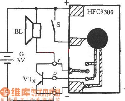
The picture above is a triode performance quick test circuit. In the picture, HFC9300 is a musical integrated circuit with a piece of music stored. BL is the speaker, and S is the triggering switch. VTx is triode under test. Insert it in a socket and insert the collector of the base in into ‘c’, the base into ‘b’ and emitter into ‘e’. If theVTx wokrs, BL would play a piece of touching music; otherwise, BL would give out no sound. (View)
View full Circuit Diagram | Comments | Reading(670)
complementary tube monostable circuit
Published:2011/6/30 6:35:00 Author:Fiona | Keyword: complementary tube, monostable
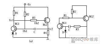
Picture shows the two forms of complementary tube monostable circuit, Figure (b) is complementary tube monostable circuit which the two tubes keep saturation in ordinary state. When it meets conditions,R2 <β1,R1 and R3 <β2, R4,the circuit is in two tubes steady states,when the negative pulse is used at the base BG1, BG1 is out of saturation, and causes a reaction Uc1 ↑ → Ub2 ↑ → Uc2 ↓ → Ub1 ↓.The result of a positive feedback chain reaction is that BG1, BG2 are closed, this is the temporary steady state.At this point C discharges to power supply through R2, R4,it enters two tube saturated stable state after discharging.Diode D is to prevent voltage of C puncturing BG1's base - emitter junction, the pulse width is:
tr=0.7(R2+R4)C
(View)
View full Circuit Diagram | Comments | Reading(1115)
Deep well water level probing and sucking device circuit diagram
Published:2011/6/25 10:46:00 Author:Vicky | Keyword: water level probing and sucking device
The circuit as shown in the above picture is composed of conductive sensor probe, electronic switch circuit, silicon-controlled control-motor circuit, croak-sounding circuit and AC brownout rectifying circuit. Its circuit is simple and It is very easy to test the water level and suction in a deep well. (View)
View full Circuit Diagram | Comments | Reading(1476)
Ultrasonic Remote Switch Obbligato Sounding Circuit Diagram
Published:2011/6/25 10:45:00 Author:Vicky | Keyword: Ultrasonic Remote Switch Obbligato Sounding
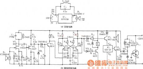
The circuit in the above picture is composed by ultrasonic remote transmitter (picture a) and receiving and controlling sections. The circuit adpts 40KHz ultrasonic signal as the remote control command, with a effecting range of no less than 25m2. (View)
View full Circuit Diagram | Comments | Reading(670)
Block Circuit Diagram of Internal LM567CN Integrated Circuit
Published:2011/6/15 8:20:00 Author:Vicky | Keyword: Block Circuit Diagram
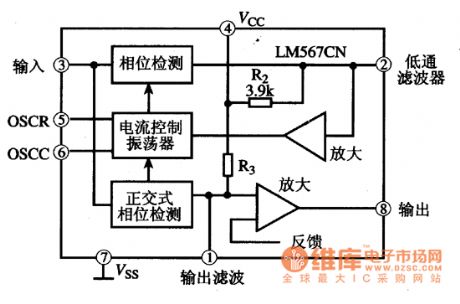
LM567CN is a PLL audio coding integrated circuit. A high-powered cordless phone often uses two pieces of this circuit, taking charge of identifying pilot frequency signal when mobile is off hook and calling signal of the mobile to host machine respectively. (View)
View full Circuit Diagram | Comments | Reading(1179)
Typical Applied Circuit Diagram of LM567CN Integrated Circuit
Published:2011/6/15 8:19:00 Author:Vicky | Keyword: Typical Applied Circuit Diagram
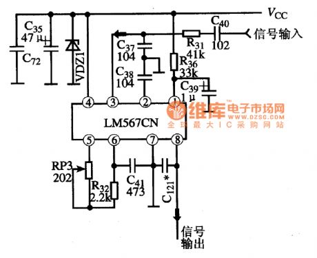
Typical Applied Circuit
Typical applied circuit of decoding circuit, which is composed of LM567CN Integrated Circuit, is shown in the following picture.
(View)
View full Circuit Diagram | Comments | Reading(3393)
Capacitance Charge and Discharge Demonstrator Circuit Diagram
Published:2011/6/15 8:21:00 Author:Vicky | Keyword: Capacitance Charge and Discharge Demonstrator
Capacitance Charge and Discharge Demonstrator is mainly used to demonstrate the changing of the curves of voltage at the two ends of the capacitance and the discharge current as the pass of time when the capacitance is in the processions of charging and discharging. The following picture is a demonstration circuit. It adopts the way of displaying by the luminosity aroused by flow of the luminous diode, and it is vivid and visual , and very close to the actual procession of charging or discharging , which is of great practical value. (View)
View full Circuit Diagram | Comments | Reading(712)
Typical Appied Circuit Diagram of LM1036N Integrated Circuit
Published:2011/6/15 8:15:00 Author:Vicky | Keyword: Typical Applied Circuit Diagram
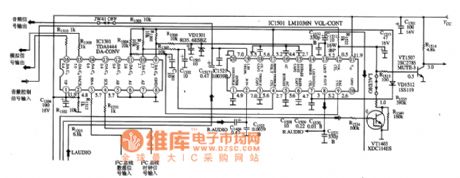
Picture: Typical Applied Circuit of LM1036N Integrated Circuit
Typical Applied Circuit
Typical Appied Circuit Diagram of LM1036N Integrated Circuit is as shown in the picture. (View)
View full Circuit Diagram | Comments | Reading(2117)
Internal Circuit Block Circuit Diagram of LM1203 Integrated Circuit
Published:2011/6/15 8:15:00 Author:Vicky | Keyword: Internal Circuit Block Circuit Diagram
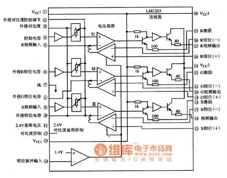
Picture:Internal CircuitBlock Circuit Diagram of LM1203 Integrated Circuit
Functions and Characteristics
The interior of LM1203 integrated circuit is made of three circuits of the same functions, including video small-signal processing circuit, contrast basic control circuit and clamp pulse, and some other adjunct circuits. The internal circuit block diagram is as shown in the picture. (View)
View full Circuit Diagram | Comments | Reading(1323)
the circuit of constant temperature controller for fish breeding(2)
Published:2011/6/15 7:18:00 Author:Ariel Wang | Keyword: constant, temperature, controller, fish, breeding
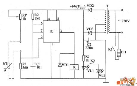
When the temperature of water is lower than the set temperature,the value of RT's resistence increases.The voltage of pin-2 of IC is lower than Vcc/3.Pin-3 of IC outputs high level.K is conducted to pull in.The normally open contacts K1 is conducted.The electric heater EH is conducted to work.Heating indicator LED VL2 is lighted.As the temperature of water goes up and up,the value of RT's resistence decreases.When the temperature of water goes beyond the setwater temperature,the voltage of IC's pin-2 is beyond Vcc/3.The voltage of Pin-3 becomes low level from high level.K is released.EH is power-off.And it stopes heating.V12 goes out of light.It goes on and on.Then the temperature of water can stay around the set temperature. (View)
View full Circuit Diagram | Comments | Reading(549)
One Digit Random Number Generator Circuit Diagram
Published:2011/6/15 8:14:00 Author:Vicky | Keyword: One Digit Random Number Generator
Random Number Generator is a digital generator which is not controlled by men's will.Thereforeit is fair and just to use it as Ernie (electronic random number indicator equipment). The working principle of random number generator is as shown in the picture. (View)
View full Circuit Diagram | Comments | Reading(2921)
| Pages:1600/2234 At 2015811582158315841585158615871588158915901591159215931594159515961597159815991600Under 20 |
Circuit Categories
power supply circuit
Amplifier Circuit
Basic Circuit
LED and Light Circuit
Sensor Circuit
Signal Processing
Electrical Equipment Circuit
Control Circuit
Remote Control Circuit
A/D-D/A Converter Circuit
Audio Circuit
Measuring and Test Circuit
Communication Circuit
Computer-Related Circuit
555 Circuit
Automotive Circuit
Repairing Circuit