
Oscillator Circuit
Index 22
_VOLTAGE_TUNED_VHF_OSCILLATOR
Published:2009/7/11 4:08:00 Author:May
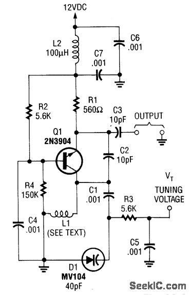
This VHF VCO circuit is suitable for 30 to 200 MHz. Q1 can be replaced by a 2N3563 for operation above 100 MHz. L1 is chosen to resonate to the desired frequency with the varactor capacitance of 40 pF. Other vatactors can be substituted or two back-to-back vat-actors can be used for better linearity, depending on the application. (View)
View full Circuit Diagram | Comments | Reading(2584)
LINEAR_VCO
Published:2009/7/11 4:02:00 Author:May
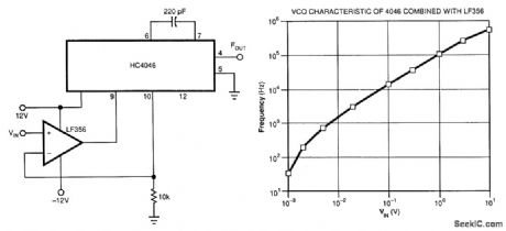
This VCO uses an LF356 op amp to produce a linear frequency vs. voltage characteristic using the CMOS HC4046. The frequency range can be changed by changing the capacitor connected between pins 6 and 7 of the HC4046. Using the HC4046's internal transistor instead of an external component achieves the linearization in Fig. 98-5(b). (View)
View full Circuit Diagram | Comments | Reading(3351)
SIMPLE_555_VCO
Published:2009/7/11 3:59:00 Author:May
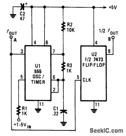
The VCO has an output frequency that ranges from 1 500 Hz at Vin=1 V to 300 Hz at Vin=5V. R1 or C1 can be varied to change this range. U2 provides a symmetrical square-wave output of half the timer frequency. (View)
View full Circuit Diagram | Comments | Reading(1400)
__RESTRICTED_RANGE_VCO
Published:2009/7/11 3:57:00 Author:May

This VCO is adjustable from 60 Hz to 1.4 kHz. C1 can be changed for other ranges (View)
View full Circuit Diagram | Comments | Reading(1301)
__GATED_WIDE_RANGE_VCO
Published:2009/7/11 3:49:00 Author:May
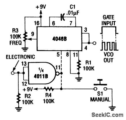
A CD4046 can be gated either with a switch or electronically, as shown in the figure. Frequency range of this circuit is to 1.5 kHz; use another C1 for higher frequencies. (View)
View full Circuit Diagram | Comments | Reading(1315)
SIMPLE_AUDIO_FREQUENCY_VCO
Published:2009/7/11 3:47:00 Author:May
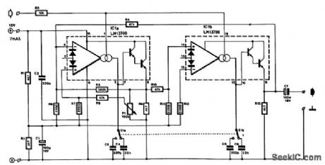
The frequency of this sine-wave oscillator is determined by a direct voltage, UC, of 0 to 15 V. The distortion on output signals of up to 10 Vpp is not greater than 1%. When the output is reduced with the aid of Pl to 1 Vpp, the distortion drops to below 0.1% It is not recommended to use output signals below 1 Vpp, because the oscillator then becomes unstable and temperature-dependent.The oscillator consists of two operational transconductance amplifiers (OTAs) contained in one package. Their Amp-bias inputs, pins 1 and 16, are connected in parallel. These inputs can drive the output currents at pins 5 and 12 to a peak value of up to 0.75 mA.Switch S1 enables the oscillator output to be set to two ranges: 6.7 to 400 Hz and 400 Hz to 23.8 kHz.The overall range needs a control voltage that varies from 1.34 to 15 V. When the frequency is changed by a variation of UC and the setting of P1 is not altered, the output signal might be distorted. In other words, the amplitude of the signal must be adapted to the frequency. (View)
View full Circuit Diagram | Comments | Reading(2227)
KEYER_OSCILLATOR
Published:2009/7/11 3:24:00 Author:May
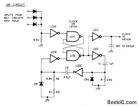
Oscillator or clock starts when key is closed and can be held until dot, dash, or space is completed. U1 is SN7400, and U2 is SN74L04. Diodes at input of U2A form OR gate that controls oscillator. These inputs can be used to keep oscillator running for self-completing action. Time constant, set by C1 and R1, is 4 ms which is width of clock pulse. Values for C2, R2, and R3 give pulse repetition rate of 50 to 95 ms, comesponding to about 12 to 24 WPM.For higher speeds, reduce values of C2 and R2.CR1 and CR2 are signal diodes that prevent first pulse from being different; 250-pF capacitor on output prevents noise spikes from triggering keyer circuits falsely.-J. T. Miller, Integrated-Circuit Oscillator, Ham Radio, Feb. 1978, p 77. (View)
View full Circuit Diagram | Comments | Reading(1500)
SIDEREAL_REGENERATIVE_OSClLLATOR
Published:2009/7/11 3:19:00 Author:May
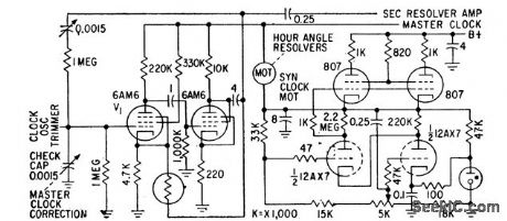
Compares synchronous clock motor speed at 30-sec intervals with pendulum-driven master sidereal-time clock. Motor runs slightly faster than sidereal lime. If too fast at checking time, check capacitor at input of V1 is closed to reduce frequency of oscillation ond speed of motor to bring it back into coinddence with master.-C.N. Kingston, Radio Telescope Sees 2 Billion Light Years, Electronics, 31:23, p70-75. (View)
View full Circuit Diagram | Comments | Reading(799)
10_MC_CLOCK_OSCILLATOR
Published:2009/7/11 3:02:00 Author:May

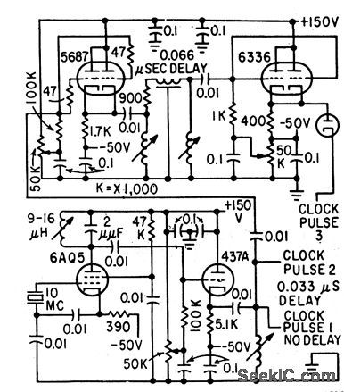
Output through cathode follower is split into three channels(two are not shown) to get clock pulses at three phases.-G,O. Olson,Design of High-Frequency clock Pulse Generators Electronics,32:35,p56-57. (View)
View full Circuit Diagram | Comments | Reading(685)
809_11_KC_CLOCK_OSCILLATOR
Published:2009/7/11 2:41:00 Author:May
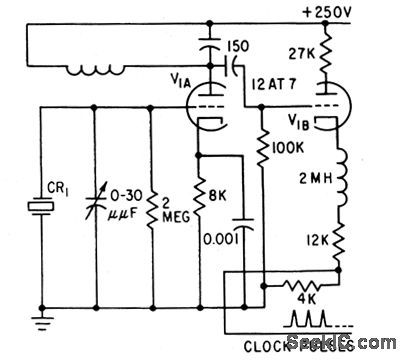
Crystctl-controlled oscillator V1A and shaping circuit V1B produce pulses with repetition rate equal to frequency of crystal oscillator.-H. Vantine Jr.and E. C. Johnson, Modified Transceivers Compute Distance, Electronics, 31:37, p94-98. (View)
View full Circuit Diagram | Comments | Reading(816)
AF_OSCILLATOR_MONITORS_CW
Published:2009/7/11 2:29:00 Author:May
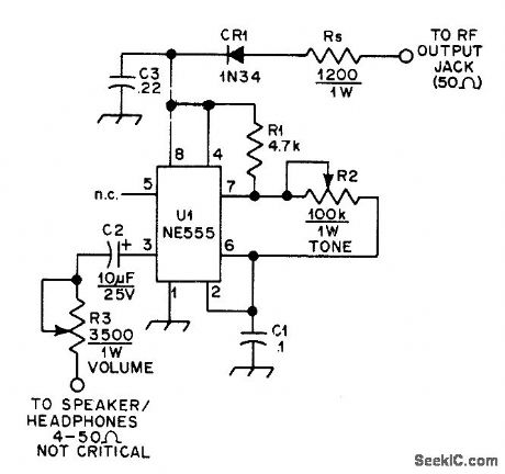
Can be added to any transceiver not already having built-in sidetone oscillator, to hear keying of transmitter. RF input from transmitter is rectified by CR1 to provideabout 6-VDC supply. Keying of carrier on and off tums NE555 AF oscillator on and off correspondingly.-J. Amold, A CW Monitorfor the Swan 270, QST, Aug. 1976, p 44. (View)
View full Circuit Diagram | Comments | Reading(1180)
CLOCK_OSCILLATOR
Published:2009/7/11 2:18:00 Author:May
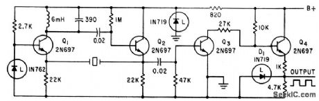
Q11 and Q2 form oscillator section of tim-base generator, and Q3-Q4 serve as pulse shaper. Q1 is grounded-base voltage amplifier with tuned collector load.Q2 matches impedance of Q1 collector circuit to crystal. Output amplitude is limited by zener diode D1-R.S. Reed,Rugged Arming-Fuzing Timer for Atomic Artillery Mssile Electronics,34:38,p48-51. (View)
View full Circuit Diagram | Comments | Reading(998)
Triangular_square___wave_VCO
Published:2009/7/17 3:17:00 Author:Jessie
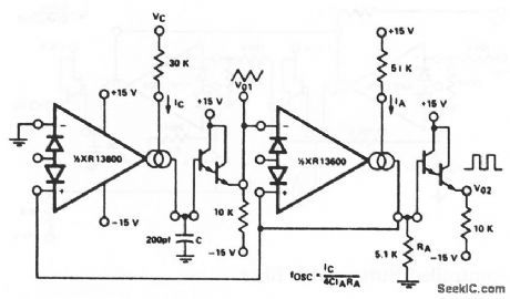
This classic triangular/square-wave generator (chapter 5) uses both sections of an XR-13600 (Fig. 11-1B). With the values shown, the oscillator provides signals from 200 kHz to below 2 Hz when IC is varied from 1 mA to 10 nA.The output amplitudes are set by IA×RA. Notice that the peak differential-input voltage must be less than 5 V to prevent zenering the inputs. EXAP Corporahon Databook 1990 p 5-255 (View)
View full Circuit Diagram | Comments | Reading(959)
SSB_COHERENT_RADAR_OSCILLATOR
Published:2009/7/17 3:07:00 Author:Jessie

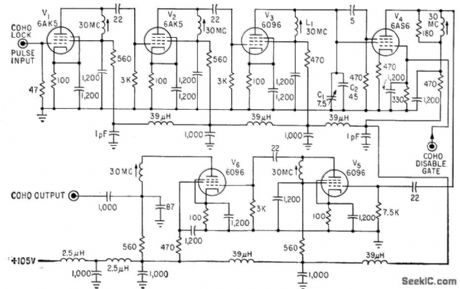
Phase information of each transmitted pulse is stored in coherent oscillator V3 for use as reference voltage for analyzing doppler return from targets. Other stages are amplifiers. Oscillator lank is L1-C1-C2. This oscillator has good free-running stability and is easily locked in phase with 30.Mc input pulse.-J. B. Theiss, More Target Data with Sideband Coherent Radar, Electronics, 36:3, p 40-43. (View)
View full Circuit Diagram | Comments | Reading(1076)
TRANSlSTOR_TESTlNG_OSClLLATOR
Published:2009/7/11 1:41:00 Author:May

With any good general-purpose transistor, circuit delivers steady AF tone to earphone. To test another transistor, substitute it in appropriate socket. No tone means it is bad. Low tone or chirp indicates questionable condition. If type (PNP or NPN) is unknown, try in both sockets. If leads of unknown cannot be identified, try all three possible positions in socket.-Circuits, 73 Magazine, July 1977, p 35. (View)
View full Circuit Diagram | Comments | Reading(755)
One_shot_multivibrator_using_an_ECG955M_timer_oscillator_chip
Published:2009/7/17 4:09:00 Author:Jessie
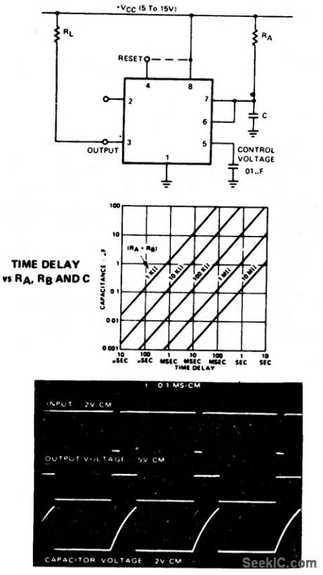
One-shot multivibrator using an ECG955M timer/oscillator chip. Upon application of a negative trigger to pin 2 the flip-flop is set, which releases the short circuit across the external capacitor. This dives the output high. The photo shows the actual waveforms generated in this mode. The time that the output is high is given by t= 1.1 RA C and can be easily determined by the graph showing time delay. Applying a negative pulse to reset terminal 4 cluing the timing cycle discharges the capacitor and causes the cycle to start again. When the reset function is not used it is recommended that it be connected to supply voltage to avoid false triggering (courtesy GTE Sylvania Incorporated). (View)
View full Circuit Diagram | Comments | Reading(934)
Ionization_chamber_smoke_detector_using_discrete_transistors_for_alarm_oscillators
Published:2009/7/17 4:01:00 Author:Jessie
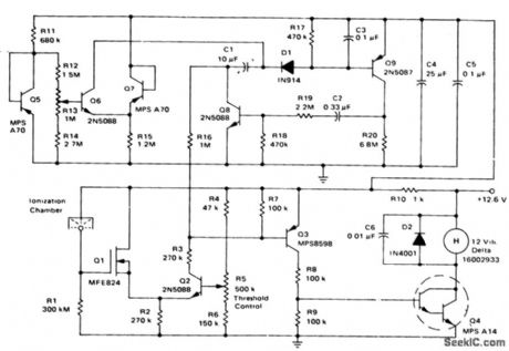
Ionization-chamber smoke detector using discrete transistors for alarm oscillators(Courtesy Motorola Semiconductor Products Inc.). (View)
View full Circuit Diagram | Comments | Reading(1298)
Norton_square_wave_oscillator
Published:2009/7/17 4:26:00 Author:Jessie
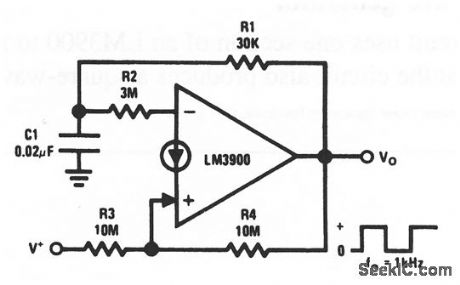
This circuit uses one section of an LM3900 to form a square-wave oscillator (with a 1-kHz output using the values shown). National Semiconductor Linear Applications Handbook 1991 p 232 (View)
View full Circuit Diagram | Comments | Reading(926)
Norton_sine_wave_oscillator
Published:2009/7/17 4:26:00 Author:Jessie
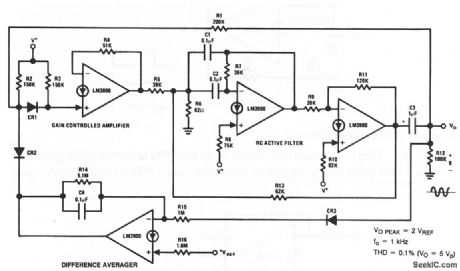
This circuit uses four sections of an LM3900 to form a sine-wave oscillator. One section is used as a gain-controlled amplifier (to sustain feedback), and another section is a difference averager that maintains a constant output level.The remaining sections are connected as an RC active filter (to produce a 1-kHz output with the values shown). National Semiconductor Linear Applications Handbook 1991 p 231 (View)
View full Circuit Diagram | Comments | Reading(1149)
BLOCKING_OSCILLATOR_FOR_10_1_SYNC
Published:2009/7/19 21:04:00 Author:Jessie
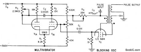
Combines basic mvbr and blocking oscillator into self-gated oscillator that gives synchronization ratio of 10:1 or greater, with stability equal to that of conventional circuit having 1:1 synchronization.-W. W. Whatley Blocking Oscillator for Ten-to-One Sychronization, Electronics, 32:48, p 58-59. (View)
View full Circuit Diagram | Comments | Reading(870)
| Pages:22/54 At 202122232425262728293031323334353637383940Under 20 |
Circuit Categories
power supply circuit
Amplifier Circuit
Basic Circuit
LED and Light Circuit
Sensor Circuit
Signal Processing
Electrical Equipment Circuit
Control Circuit
Remote Control Circuit
A/D-D/A Converter Circuit
Audio Circuit
Measuring and Test Circuit
Communication Circuit
Computer-Related Circuit
555 Circuit
Automotive Circuit
Repairing Circuit