
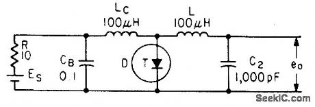
Oscillator Circuit
Index 29
VARIABLE_AMPLITUDE_TUNNEL_DIODE_OSCILLATOR
Published:2009/7/20 2:07:00 Author:Jessie
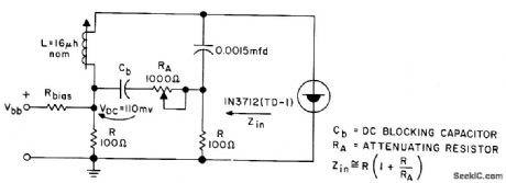
Attenuating resistor RA varies magnitude of oscillator swing, so oscillator operates over limited highly linear portion of diode conductance curve.- Transistor Manual, Seventh Edition, General Electric Co., 1964, p 351. (View)
View full Circuit Diagram | Comments | Reading(1005)
SINE_WAVE_TUNNEL_DIODE_1
Published:2009/7/20 2:05:00 Author:Jessie
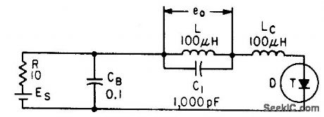
Series filter selects desired frequency and rejects harmonics from pulse-shaped output of basic tunnel-diode relaxation oscillator. Values shown give 0.45 Mc, constant within 0.05 Mc over bias range of 100 to 400 mv.-Wen-Hsiung Ko, Designing Tunnel Diode Oscillators, Electronics, 34:6, p 68-72. (View)
View full Circuit Diagram | Comments | Reading(792)
471_MC_TUNNEL_DIODE_CRYSTAL_OSCILLATOR
Published:2009/7/20 2:04:00 Author:Jessie
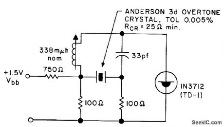
Used in Fire Department service. 0perates within tolerance of quartz crystal from -55 to +85℃ and bias range of 110 to 150 mv for Citizens Band service.- Transistor Manual, Seventh Edition, General Electric Co., 1964, p 353. (View)
View full Circuit Diagram | Comments | Reading(1162)
CRYSTAL_OR_CAPACITOR_OSCILLATOR
Published:2009/7/20 2:02:00 Author:Jessie
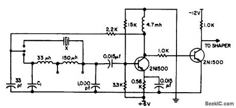
Gives high stability from 800 kc to 3 Mc, from 0 to 65℃ with either crystal or capacitor. Optimum operating frequency can be found and utilized by changing capacitor value C1 in range up to 500 pf, while awaiting delivery of CT-cut crystal at desired frequency. -T. Asai, Crystal-or-capacitor Oscillator, EEE, 12:3, p 72. (View)
View full Circuit Diagram | Comments | Reading(855)
SINE_WAVE_TUNNEL_DIODE
Published:2009/7/20 2:01:00 Author:Jessie
Low-impedance capacitor in parallel with sefies-resonant circuit of tunnel-diode relaxation oscillator passes all frequencies except that for series resonance, giving sinusoidal voltage across output capacitor. Output frequency varies from Q1 to 0.8 Mc over bias range of 000 to 400 mv.-Wen-Hsiung Ko, Designing Tunnel Diode Oscillators, Electronics, 34:6, p 68-72. (View)
View full Circuit Diagram | Comments | Reading(1275)
100_MC_COLPITTS
Published:2009/7/20 2:00:00 Author:Jessie
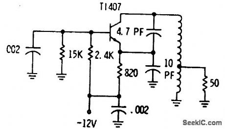
Uses conventional bipolar transistor, which has low noise in operation from low-impedance voltage generator. Temperature drift is much greater than with fet. -Fets Come Alive: Clinic Unveils Practical Circuits, EEE, 14:4, p 16-18. (View)
View full Circuit Diagram | Comments | Reading(821)
FET_HARTLEY
Published:2009/7/20 1:59:00 Author:Jessie
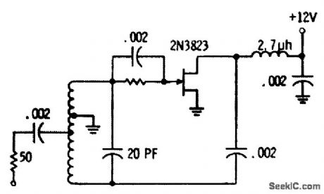
Delivers 680 mv to 50-ohm load at 100 Mc. Coil is four 3/8-inch-diameter turns of No. 16 wire spaced to 0.5 inch.-Fets Come Alive: Clinic Unveils Practical Circuits, EEE, 14:4, p 16-18. (View)
View full Circuit Diagram | Comments | Reading(933)
WIEN_BRIDGE_OSCILLATOR_CIRCUIT
Published:2009/7/20 4:22:00 Author:Jessie

A 741 op amp is connected to a Wien-bridge, audio-sine-wave oscillator configuration, with C1, C2, R1, and R2 determining the circuit's operating frequency. With the use of NPO capacitors and metal-film resistors, the oscillator's frequency is stable enough for use in tone-control applications. The fixed-frequency oscillator shown can easily be converted into a tunable oscillator by substituting a dual-gang linear potentiometer for R1 and R2. Different frequency ranges can be covered by using other matched values for C1 and C2. Larger values produce lower frequencies, and vice versa for small values. (View)
View full Circuit Diagram | Comments | Reading(0)
THREE_FREQUENCY_AUDIO_OSCILLATOR
Published:2009/7/20 4:20:00 Author:Jessie
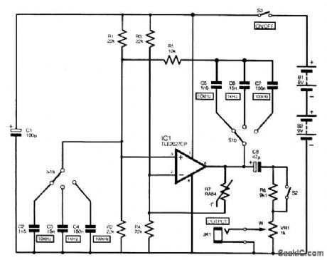
The full circuit diagram for the audio sine-wave generator is shown. Resistors R1 and R2 bias the noninverting (pin 3) input of IC1, and their parallel resistance forms one element of the Wien net-work. They are the equivalent of R1 in Fig. 1. The other resistor in the Wien network is R5. Three switched pairs of capacitors (C2 to C7) provide the unit with its three different output frequencies. Resistors R3 and R4 bias the inverting (pin 2) input of IC1, and their parallel resistance also acts as one element of the negative-feedback network. Thermistor R7 is the other section of the negative-feedback circuit. An RA53 thermistor is the normal choice for this application, but because of its lower cost, an RA54 is used in this circuit. Potentiometer VR1 is the variable-output attenuator. Opening switch S2 introduces losses through resistor R6 that reduce the output by about 20 dB. Use a value of 100 kΩ for R6 if a reduction by about 40 dB is preferred. (View)
View full Circuit Diagram | Comments | Reading(2643)
THREE_TONE_OSCILLATOR
Published:2009/7/20 4:18:00 Author:Jessie
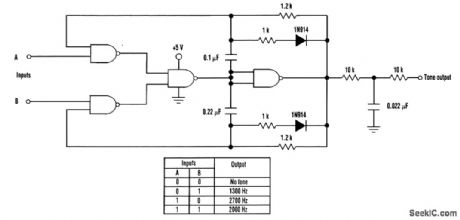
This TTL tone oscillator can generate one of three tones. The tone generation depends on the status of the two input control lines. The design consists of two standard TTL audio tone oscillators merged together using one 7400 TTL chip. Two input lines control the output status. With both inputs low, no output is generated. When input A is high, the high-tone oscillator is gated on. When input B is high, the low-tone oscillator is gated on. With both A and B high, both oscillators are gated on and the output tone generated is midway between the high and low tones. The 1N914 diode in series with a 1-kΩ resistor imposes a 50-percent duty cycle on the waveform. A low-pass filter on the output removes harmonics and mellows the output tone. (View)
View full Circuit Diagram | Comments | Reading(1873)
AUDIO_GENERATOR_CIRCUIT
Published:2009/7/20 4:17:00 Author:Jessie
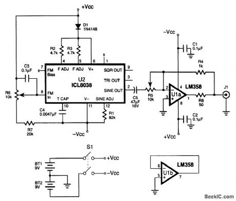
A very compact audio signal generator can be constructed using a precision waveform generator IC (ICL8038) made by Harris Semiconductor. This IC is unique in that it will generate three wave-forms: sine, triangle, and square waves. The frequency output is adjustable between 0.01 Hz and 300 kHz, and the sine-wave output distortion is less than 1 percent. The schematic diagram illustrates the application of the ICL8038 IC to construct a battery-powered mini-audio-signal generator that will provide 500 Hz to 1.5 kHz with adjustable-amplitude output. The output frequency of the generator is set by the combination of R2, R3, and (View)
View full Circuit Diagram | Comments | Reading(7090)
SIMPLE_VCO
Published:2009/7/9 4:12:00 Author:May
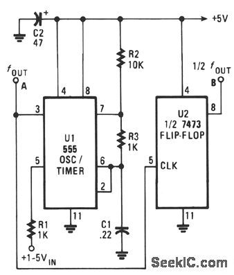
The output frequency of the VCO, U1, vanes inversely with the input voltage. With a 1-V input, the oscillator output frequency is about 1500 Hz; with a 5-V input, the output frequency drops to around 300 Hz. The output frequency range of U1 can be altered by varying the values of C1, R2, and R3. Increasing the value of any those three components will lower the oscillator frequency, and decreasing any of those values will raise the frequency. Output-waveform symmetry suffers since the frequency varies from one extreme to the other. At the highest frequency, the waveform is almost equally divided. But when the frequency drops, the output of the circuit turns into a narrow pulse. If a symmetrical waveform is required, add the second IC, U2, half of a 7473P dual TTL J-K flip-flop, to the oscillator circuit. The signal frequency output by U2 is 1/2 of the input. (View)
View full Circuit Diagram | Comments | Reading(1068)
VCO
Published:2009/7/9 4:08:00 Author:May

At startup, the voltage in the trigger input at pin 2 is less than the trigger level voltage, 1/3 VDD, causing the timer to be triggered via pin 2. The output of the timer at pin 3 becomes high, allowing capacitor Ct to charge very rapidly through diode D1 and resistor R1.When capacitor Ct charges to the upper threshold voltage 2/3 VDD, the flip-flop is reset, the output at pin 3 decreases, and capacitor Ct discharges through the current mirror, TL011. When the voltage at pin 2 reaches 1/3 VDD, the lower threshold or trigger level, the timer triggers again and the cycle is repeated. (View)
View full Circuit Diagram | Comments | Reading(1422)
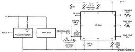
LOGARITHMIC_SWEEP_VCO
Published:2009/7/9 3:58:00 Author:May
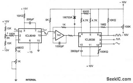
This circuit uses the output of the ICL8049 to control the frequency of the ICL3038 waveform genera-tor; the 741 op amp is used to linearize the voltage-frequency response. The input voltage to the 8049 can be, for example, from the horizontal sweep signal of an oscilloscope; the output of the 8038 will then sweep logarithmically across the audio range. By feeding this to the equipment being measured and detecting the output, a standard frequency response can be obtained. If the output is fed through an ICL8048 before being displayed, a standard bode plot results. (View)
View full Circuit Diagram | Comments | Reading(2158)
VARIABLE-CAPACITANCE_DIODE_SPARKED_VCO
Published:2009/7/9 3:52:00 Author:May
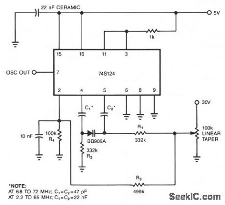
You can transform a 741S124 multivibrator into a wideband VCO by replacing it conventional ftxed capacitor with a variable-capacitance diode. The only disadvantage of this scheme is the 30-V biasing volt-age that the diode requires. Capacitors C1 and C2 couple the Philips BB909A variable-capacitance diode to the 74S124. R1 and R2 are large enough to isolate ground and control voltages from the timing capacitors. Resistors R3 and R4 form a voltage divider for the 74S124's control input. (View)
View full Circuit Diagram | Comments | Reading(1229)
WAVEFORM_GENERATOR_STABLE_VCO
Published:2009/7/9 3:49:00 Author:May
In this circuit, a waveform generator is used as a stable VCO in a Phase-Locked Loop (PLL). (View)
View full Circuit Diagram | Comments | Reading(1228)
COMPUTER_SPEECH_SYNTHESIZER
Published:2009/7/9 3:25:00 Author:May
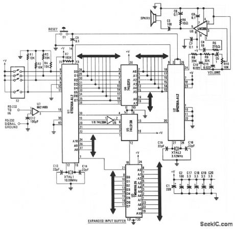
This text-to-speech converter is built around the SPO256-AL2 speech processor and the CT6256-AL2 text-to-speech converter chips-manufactured by General Instruments. The circuit is set up to receive standard ASCII code from virtually any microcomputer or dumb terminal that is equipped with an RS-232 port-such as a serial-printer or modem port. If a microcomputer is used, the synthesizer can be activated from a terminal-emulator of any communications proaram, or front any programming language such as BASIC.The serial input from the RS-232 port enters the circuit through U7, the MC1489 RS-232 receiver chip, and is converted from an RS-232 level to a TTL-level signal. The CTS256-AL2 chip, U1, then converts the ASCII characters into allophone codes and sends those codes to U3, the TMS4016 external-RAM chip. The codes are then transferred to the SPO256-AL2, U2, through the 74LS373 octal latch, U4. Finally, the SPO256-AL2 sends out an audio signal to the LM386 audio amplifier, U8, through some highpass filtering, and on to the speaker. The 74LS138d, US, and the 74LSO4, U6, provide control logic. (View)
View full Circuit Diagram | Comments | Reading(3287)
OSCILLOSCOPE_COUNTER_PREAMPLIFIER
Published:2009/7/9 2:04:00 Author:May
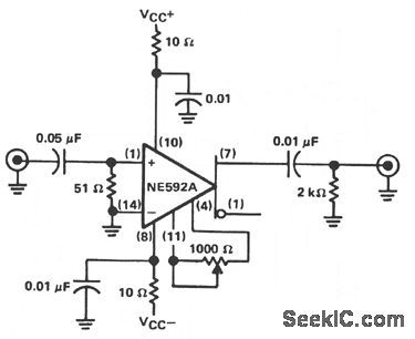
The circuit will provide a 20±0.1 dB voltage gain from 500 kHz to 50 MHz. The low-frequency response of the amplifter can be extended by increasing the value of the 0.05-μF capacitor connected in series with the input terminal. This circuit will yield an input-noise level of approximately 10 μV over a 1 5. 7-MHz bandwidth. The gain can be catibrated by adjusting the potentiometer connected between pins 4 and 11. The 1-KΩ potentiometer can be adjusted for an exact voltage gain of 10. This preserves the scale factor of the instrument. (View)
View full Circuit Diagram | Comments | Reading(893)
OSCILLOSCOPE_CALIBRATOR
Published:2009/7/9 1:59:00 Author:May
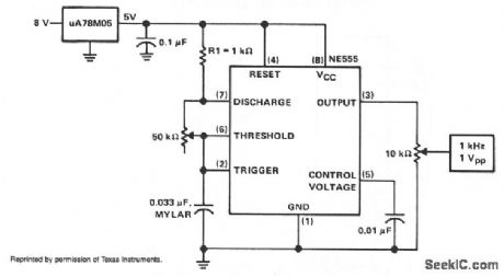
The calibrator can be used to check the accuracy of a time-base generator, as well as to calibrate the input level of amplifiers. The calibrator consists of an NE555 connected in the astable mode. The oscillator is set to exactly 1 kHz by adjusting potentiometer P1 while the output at pin 3 is being monitored against a known frequency standard or frequency counter. The output level, likewise, is monitored from potentiometer P2's center arm to ground with a standard instrument. P2 is adjusted for 1 V pk-pk at the calibrator output terminal. During operation, the calibrator output terminal will produce a 1-kHz, square-wave signal at 1 V pk-pk with about 50% duty cycle. For long-term oscillator frequency stability, C1 should be a low-leakage mylar capacitor. (View)
View full Circuit Diagram | Comments | Reading(1010)
LOW_VOLTAGE_WIEN_BRIDGE_OSCILLATOR
Published:2009/7/9 1:52:00 Author:May
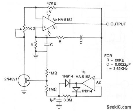
This circuit utilizes an HA-5152 dual op amp and FET to produce a low-voltage, low-power, Weinbridge sine-wave oscillator. Resistors R and capacitors C control the frequency of oscillation; the FET, used as a voltage-controlled resistor, maintains the gain of A1 exactly 3 dB to sustain oscillation. The 20-KΩ pot can be used to vary the signal amplitude. The HA-5152 has the capability to operate from ±1.5-V supplies. This circuit will produce a low-distortion sine-wave output while drawing only 400 uA of supply current.
(View)
View full Circuit Diagram | Comments | Reading(1227)
| Pages:29/54 At 202122232425262728293031323334353637383940Under 20 |
Circuit Categories
power supply circuit
Amplifier Circuit
Basic Circuit
LED and Light Circuit
Sensor Circuit
Signal Processing
Electrical Equipment Circuit
Control Circuit
Remote Control Circuit
A/D-D/A Converter Circuit
Audio Circuit
Measuring and Test Circuit
Communication Circuit
Computer-Related Circuit
555 Circuit
Automotive Circuit
Repairing Circuit