
Oscillator Circuit
Index 32
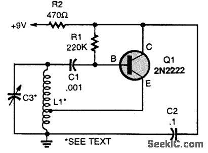
TWIN_TEE_TONE_OSCILLATOR
Published:2009/7/21 2:09:00 Author:Jessie
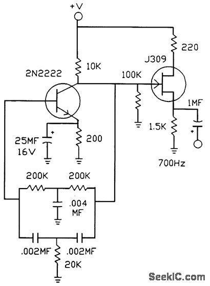
A 2N2222 transistor is used in a twin-tee oscillator, followed by a FET buffer circuit. (View)
View full Circuit Diagram | Comments | Reading(1552)
UJT_OSCILLATOR
Published:2009/7/21 2:11:00 Author:Jessie
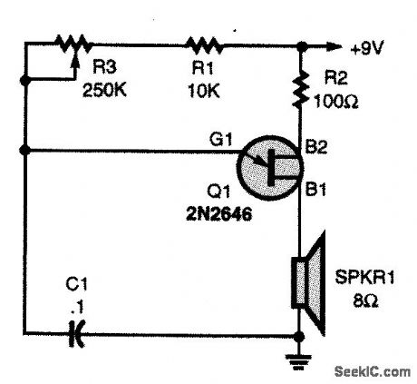
When power is connected to the circuit, C1 charges through R1 and R3. When the voltage reaches the UJT gate's (G) threshold voltage (usually around 0.5 to 0.8 of the supply voltage), the dynamic resistance between B2 and B1 drops to a very low value. Capacitor C1 then discharges through the emitter-base junction and the 8-Ω speaker. The frequency of the UJT oscillator is determined by the values of C1, R1, and R3. (View)
View full Circuit Diagram | Comments | Reading(1019)
NE602_HARTLEY_VFO_CIRCUIT
Published:2009/7/21 2:12:00 Author:Jessie
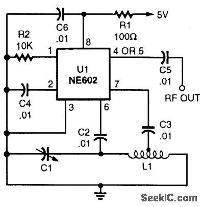
In this circuit, L1 is tapped at about one-third to one-fourth from the ground end. L1 is about 10/f MHz, while C1 is chosen to resonate L1 to the desired frequency. (View)
View full Circuit Diagram | Comments | Reading(1533)
WIDE_RANGE_OSCILLATOR
Published:2009/7/9 1:31:00 Author:May
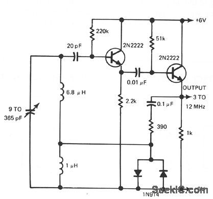
The gain control allows the oscillator to maintain essentially constant output over its range. The circuit functions over 160 kHz to 12 MHz with essentially constant amplitude. (View)
View full Circuit Diagram | Comments | Reading(1872)
HARTLEY_OSCILLATOR
Published:2009/7/21 2:13:00 Author:Jessie
The oscillator's operating frequency is determined by the values of L1 and C3. The feedback level is determined by the location of the tap on L1, which normally will be about one-fifth to one-fourth of the total turns. As an example, the Hartley oscillator will operate in the 5-MHz range with the following LC values: L1 is 20 turns of 18 enameled copper wire close wound on a 1-inch plastic form with a tap up five turns from the bottom. Capacitor C3 can be any small variable capacitor with a maximum capacitance value of 100 pF. With the proper LC values, the Hartley oscillator can operate from audio to UHF. (View)
View full Circuit Diagram | Comments | Reading(0)
VOLTAGE_TUNED_HARTLEY_JFET_VFO
Published:2009/7/21 2:15:00 Author:Jessie
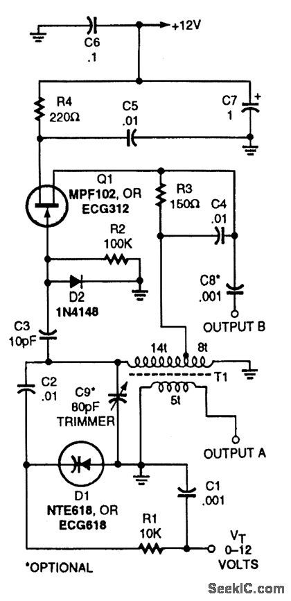
This voltage-tuned JFET Hartley oscillator can be made to sweep its entire frequency range by applying a sawtooth waveform that rises from 0 to 12 V to the Vt input. In this circuit, a varactor is used for the tuning element instead of an air-core inductor. The frequency range is around 5 MHz. (View)
View full Circuit Diagram | Comments | Reading(834)
VARIABLE_VNEN_BRIDGE_OSCILLATOR
Published:2009/7/9 1:30:00 Author:May
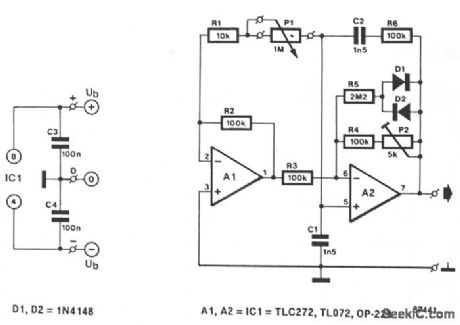
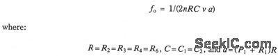
A Wien-bridge oscillator can be made variable by using two frequency-determining parts that are var-ied simultaneously at high tracking accuracy. High-quality tracking potentiometers or variable capacitors are, however, expensive and difficult to obtain. To avoid having to use such a component, this oscillator was designed to operate with a single potentiometer. The output frequency, f0,is calculated from:
With preset P2 you can adjust the overall amplification so that the output signal has a easonably stable amplitude, 3.5 VPP max., over the entire frequency range. The stated components allow the frequency to be adjusted between 350 Hz and 3.5 kHz. (View)
View full Circuit Diagram | Comments | Reading(1667)
MODIFIED_HARTLEY_OSCILLATOR
Published:2009/7/21 2:15:00 Author:Jessie
A. F. Lampkin, in 1939, showed that a high-C Hartley oscillator (as typically used in the once popular ECO VFO) could be improved by a factor of about 10 times simply by tapping the grid (gate or base) connection down the coil. (View)
View full Circuit Diagram | Comments | Reading(0)
NE602_HARTLEY_OSCILLATOR
Published:2009/7/21 2:16:00 Author:Jessie
In this Hartley VFO, feedback is provided via a tap on the inductor. (View)
View full Circuit Diagram | Comments | Reading(843)
HARTLEY_JFET_OSCILLATOR
Published:2009/7/21 2:19:00 Author:Jessie
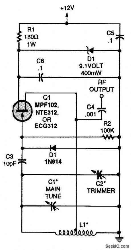
This simple Hartley JFET oscillator has a built-in zener-diode regulator to condition the power-supply voltage down to 9.1 V. L1 depends on the desired frequency. Typical values are C1=5 to 50pF variable, C2=100 pF plus a 3-to 30-pF trimmer, and L1=14μH (for 3.5 MHz). L1 should be mechanically rigid, should have an air core (do not use ferrite cores because of drift effects), and should have Q ≥ 200 for best stability. The tap will be typically 10 to 25 percent of the total turns. (View)
View full Circuit Diagram | Comments | Reading(1696)
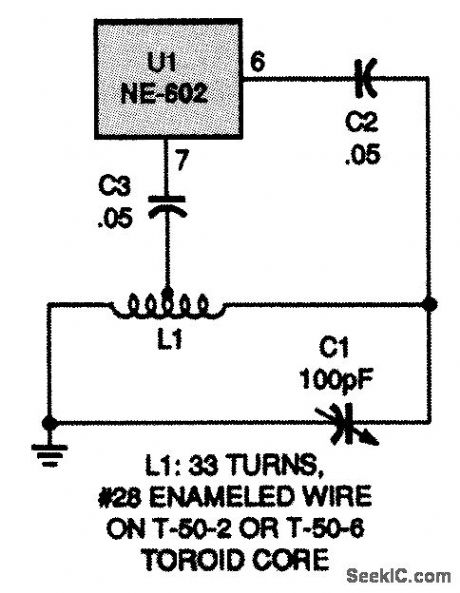
NE602_OSCILLATOR_CIRCUIT
Published:2009/7/21 2:28:00 Author:Jessie
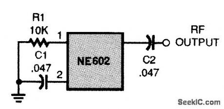
If the LO signal of the NE602 is sent directly to the output pins, the device can be used as a low-cost, high-frequency oscillator. (View)
View full Circuit Diagram | Comments | Reading(1296)
STRIP_LINE_OSCILLATOR
Published:2009/7/21 2:48:00 Author:Jessie
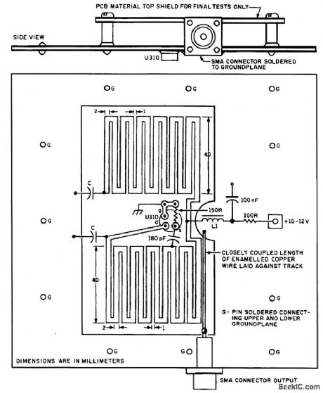
The figure shows a prototype strip tine oscillator that is capable of providing an operating range of 3.5:1 before oscillation ceases Length A∶40 mm,width B∶2 mm,width C:1 mm To change the frequency range,alter the length A and the length of the output coupling wire Typical frequencies with C=0 pF are about 145 MHz;with 27 pF, about 80 MHz; with 56 pF, about 60 MHz;and with 150 pF, about 36 MHz (plate-ceramic capacitors). With 1/16-inch double-sided PC board, note that the bottom ground plane covers the whole of the board. The output is about 0 dBm. The U310 FET is pushed through from the bottom side of the PC board until it touches the ground plane and is soldered directly to the ground plane. (View)
View full Circuit Diagram | Comments | Reading(857)
STABLE_INDUCTIVE_TUNED_OSCILLATOR
Published:2009/7/21 2:56:00 Author:Jessie

In frequency-shift keying (FSK) applications, when modulating high data rates, coupling data to the varactor can pose a problem. A duplex filter is necessary to prevent RF loading or leaking of the oscillator tank while transferring the fast data edges to the varactor. These two constraints contradict one another-especially when the edge's rise time approaches that of the carrier frequency. If an RF choke or a large-value resistor is used to inject data to the varactor, then the edges of the data will be severely distorted by RC or inductive-capacitive (LC) time constants. The loss of these rise times can result in duty-cycle distortion as seen by the threshold level detector in the receiver. To improve upon the traditional VCO techniques, varying the inductor provides increased tuning sensitivity and better resonator Q. Inductive tuning uses the coupling or leakage inductance characteristics of a transformer. Thus, tuning capacitor C4 can be changed to a fixed, high-quality capacitor. Use of a negative -temperature -coefficient capacitor here can balance out the active device's capacitance variation with temperature. The tuning inductor (L1) is now a transformer. At about 48 MHz, it is a nine-turn, center-tapped coil of AWG28 wound on a 725-10 Micrometals core. Other transformers also can be implemented, depending on operating frequencies and performance requirements. The Q for this inductor is about 100, which is more than sufficient to isolate the active device to prevent its pulling the oscillator tank over the extended temperature range of -40 to 85℃. The inductance variation or stability with temperature is dependent on the core material of L1. (View)
View full Circuit Diagram | Comments | Reading(1162)
LOW_NOISE_OSCILLATOR
Published:2009/7/21 2:57:00 Author:Jessie
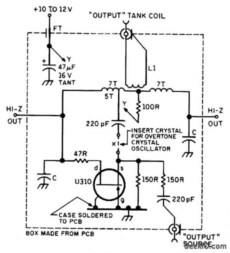
This oscillator is suitable for low-noise applications. L is wound on a 6-mm form, and C is 15 to 220 pF. The frequency range is 20 to 80 MHz. The output is 0 dBm into 50 Ω. For use of the circuit as a crystal-controlled oscillator, a crystal can be inserted as shown. (View)
View full Circuit Diagram | Comments | Reading(866)
TTL_RING_OSCILLATOR
Published:2009/7/21 2:58:00 Author:Jessie
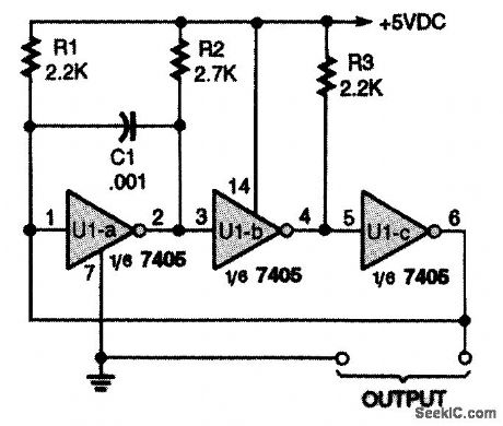
A TTL ring-oscillator circuit uses an odd number of inverters in an astable configuration. (View)
View full Circuit Diagram | Comments | Reading(919)
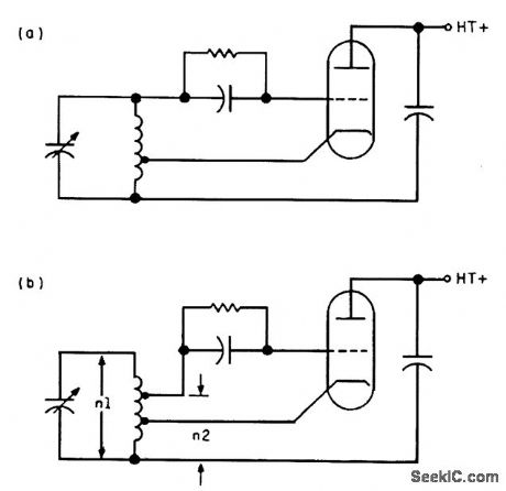
FRANKLIN_OSCILLATOR
Published:2009/7/21 2:59:00 Author:Jessie

Shown in tube form, this circuit shows the principle and the configuration of the Franklin oscillator.
The basic Franklin master oscillator, first described in 1930, uses very low-value capacitors, C1 and C2 (about 1 to 3 pF), imposing a very light load on the high-Q tuned circuit. Further advantages include the two-terminal inductance and the earthing of one end of the resonant circuit. This form of oscillator can be readily adapted for use with MOSFET devices. (View)
View full Circuit Diagram | Comments | Reading(2384)
CENTER_TAPPED_TRANSFORMER_AUDIO_OSCILLATOR
Published:2009/7/21 2:03:00 Author:Jessie
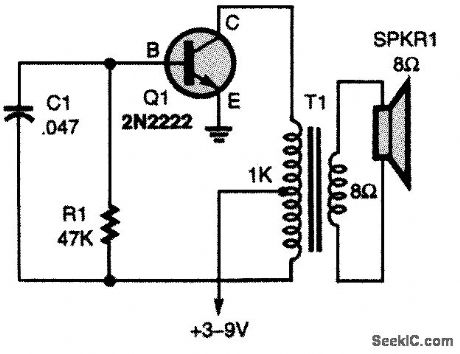
The oscillator circuit uses a center-tapped transistor output transformer to serve as a load for the collector of Q1, supply a feedback signal for the base, and serve as the output winding for driving the speaker. R1 supplies dc bias and C1 completes the ac path from the transformer to Q1's base. You can play around with the values of C1 and R1 to change the oscillator's output level and tone, but don't reduce R1's value too much or the transistor will draw excessive collector current. (View)
View full Circuit Diagram | Comments | Reading(3728)
LOW_NOISE_DC_REGULATOR_FOR_OSCILLATOR_CIRCUITS
Published:2009/7/21 3:01:00 Author:Jessie
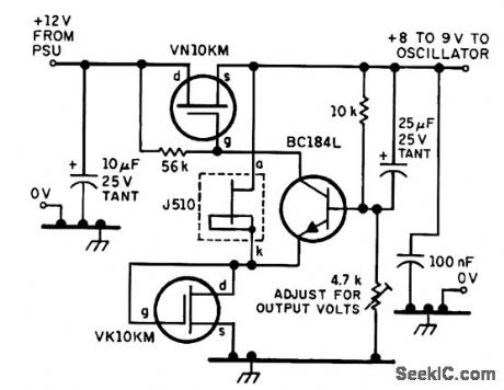
This regulator uses FET devices for low-noise dc output needed for use with variable-frequency free-running oscillators. (View)
View full Circuit Diagram | Comments | Reading(881)
18_19_MHz_VFO
Published:2009/7/8 2:15:00 Author:May
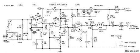

Series-tuned Clapp oscilla-torusing high-impedance JFET at has good fre-quency stability. Diode stabilizes bias. Air variable C1 provides frequency spread of exactly 100 kHz. L1 is 25-58 μH slug-tuned (Miller 43A475CBI). L2 is 10-18.7 μH slug-tuned (Miller 23A155RPC).—D. DeMaw, More Basics on Solid-State Transmitter Design, OST, Nov.1974, p 22-26 and 34. (View)
View full Circuit Diagram | Comments | Reading(1226)
LIGHT_SENSITIVE_AUDIO_OSCILLATOR
Published:2009/7/7 21:21:00 Author:May
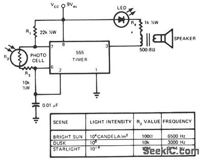
This circuit's frequency of oscillation increases directly with light intensity. The greater the light intensity, the higher the frequency of the oscillator. The 555 timer operates in the astable oscillator mode where frequency and duty cycle are controlled by two resistors and one capacitor. The capacitor charges through R1 and R2, and discharges through R2, a standard photo cell. Resistor R3 limits the upper frequency of oscillation to the audio range. The lower range of approximately 1 pps is set 'oy the value of R2, approximately 10-MΩ, with the photo cell almost totally dark.A loudspeaker provides audio output, and an LED is used as a pilot light that flashes when the frequency falls below about 10 to 12 Hz. Extremely sensitive, especially on the dark end of the photocell resistance range, the unit can detect lightning many miles away, providing a rapid frequency increase with each flash of lightning. When used with a flashlight at night, the device becomes a simple optical radar for the blind, showing angular direction to a light-reflecting object, as well as height and distance to the object when hand scanned back and forth.This light-sensitive audio oscillator can also serve as an audible horizontal level device by noting the position of a liquid bubble illuminated by a light source. Thus, you can sense fluid levels as well as the vibration state of a fluid surface level. (View)
View full Circuit Diagram | Comments | Reading(1036)
| Pages:32/54 At 202122232425262728293031323334353637383940Under 20 |
Circuit Categories
power supply circuit
Amplifier Circuit
Basic Circuit
LED and Light Circuit
Sensor Circuit
Signal Processing
Electrical Equipment Circuit
Control Circuit
Remote Control Circuit
A/D-D/A Converter Circuit
Audio Circuit
Measuring and Test Circuit
Communication Circuit
Computer-Related Circuit
555 Circuit
Automotive Circuit
Repairing Circuit