
Oscillator Circuit
Index 39
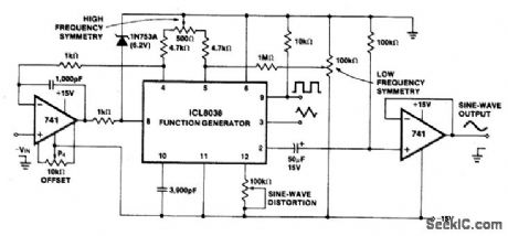
VCO_SOUND_SYNTHESIZER
Published:2009/7/2 0:43:00 Author:May
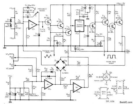
Developed for use in instrument capable of duplicating variety of sounds ranging from bird distress calls and engine noises to spoken words and wide variety of musical instruments. Three-part article gives all circuits and describes their operation in detail. Heart of oscillator is triangle and square-wave generator built around IC Schmitt trigger. Ramp rate and operating frequency are varied by changing drive voltage or gain of integrator. Similar VCO in synthesizer also produces sine, pulse, and ramp waveforms.-T. Orr and D. W. Thomas, Electronic sound synthesize, Wire-less World, part 1-Aug. 1973, p 429-434; Part 3-Oct. 1973, p 485-490. (View)
View full Circuit Diagram | Comments | Reading(974)
GATE_DIP_FET_OSCILLATOR_
Published:2009/7/1 23:51:00 Author:May
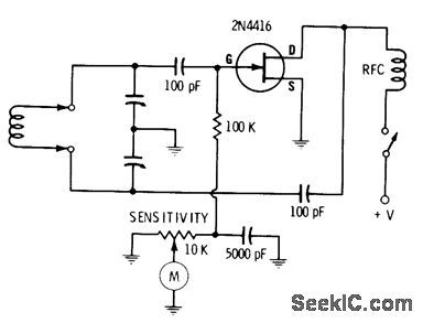
Meter indicates gate current, which drops whenever resonant load is placed on tank circuit of oscillator by bringing plug-in input coil near frequency source being checked. By opening switch to power supply, circuit can be used as absorption wavemeter; when signal at resonant frequency of dip-meter tank circuit is picked up, gatesource circuit of FET operates as diode detector for producing increase in meter reading. Values of plug-in coil and tuning capacitor depend on frequency range of interest.-E. M. Noll, FET Principles, Experiments, and Projects, Howard W. Sams, Indianapolis, IN, 2nd Ed., 1975, p 213-214. (View)
View full Circuit Diagram | Comments | Reading(3682)
GRID_DIP_OSCILLATOR
Published:2009/7/1 21:52:00 Author:May
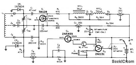
Millen 90652 solidstate grid-dip oscillator uses MOSFET operating in split-Colpitts circuit with resonating tank connected between drain and gate. Circuit is tuned by split-stator variable capacitor with rotorgrounded, chosen to cover 1.7 to 300 MHz with seven plug-in coils. Oscillator also functions as Q multiplier that increases sensitivity.RF voltage across tuned circuit is indicated by meter whose reading dips for resonance with coupled test circuit. Full-wave rectifier CR1-CR2 provides DC voltage for meter and some overload protection for MOSFET. Meter is suppressed-zero type, with readings only for upper portion of current range. J3 is provided for use with low-frequency coils.-W. M. Scherer,CQ Reviews: The Millen Model 90652 Solid-State Dipper, CQ, Sept. 1971, p 63-64, 66, and 96. (View)
View full Circuit Diagram | Comments | Reading(5114)
FET_DIP_OSCILLATOR
Published:2009/7/1 21:10:00 Author:May
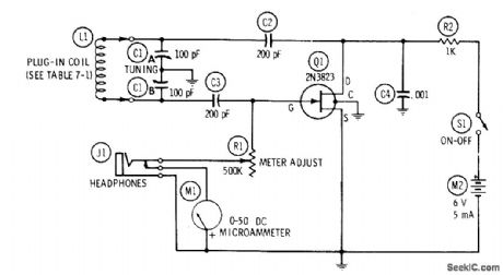
High input impedance of FET makes performance comparable to that of tube-type grid-dip oscillator. Six plug-in coils are wound on Millen 45004 1-inch 4-pin forms or equivalent. Use 150 turns No. 32 enamelfor 1.1-2.5 MHz, 77 turns No. 28 for 2.5-5 MHz, 35 turns No. 22 for 5-11 MHz, 17 turns No. 22 spaced to 1 inch for 10-25 MHz, 8.5 turns No. 22 spaced to 1 inch for 20-45 MHz and 4.5 tums No. 22 spaced to 1 inch for 40-95 MHz. Adjust R1 to set meter pointer to desired portion of scale before tuning for dip. R1 provides some control of volume when using headphones.-R.P. Turner, FET Circuits, Howard W. Sams, Indianapolis, IN, 1977, 2nd Ed., p 134-136. (View)
View full Circuit Diagram | Comments | Reading(4986)
VOLTAGE_CONTROLLED_OSCILLATOR_2
Published:2009/7/1 21:04:00 Author:May
View full Circuit Diagram | Comments | Reading(751)
VOLTAGE_CONTROLLED_OSCILLATOR_1
Published:2009/7/1 21:03:00 Author:May
View full Circuit Diagram | Comments | Reading(784)
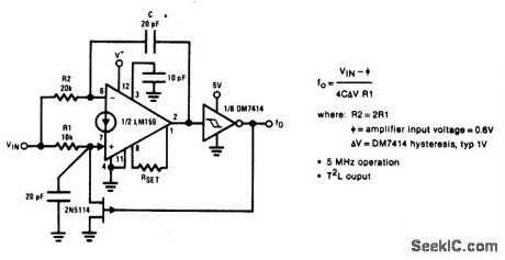
TWO_DECADE_HIGH_FREQUENCY_VCO
Published:2009/7/1 21:02:00 Author:May
View full Circuit Diagram | Comments | Reading(940)
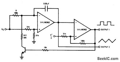
THREE_DECADES_VCO
Published:2009/7/1 21:01:00 Author:May
View full Circuit Diagram | Comments | Reading(796)
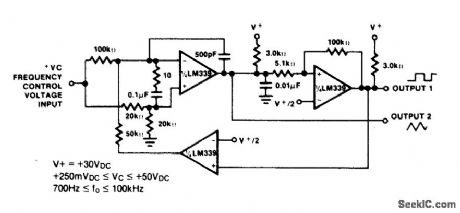
SIMPLE_VOLTAGE_CONTROLLED_OSCILLATOR
Published:2009/7/1 21:00:00 Author:May
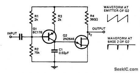
With the component values shown, the oscillator has a frequency of 8 kHz. When an input signal is applied to the base of Q1 the current flowing through Q1 is varied, thus varying the time required to charge C1. Due to the phase inversion in Q1 the direction of output frequency change is 180 degrees out of phase with the input signal. The output may be used to trigger a bistable flip-flop. (View)
View full Circuit Diagram | Comments | Reading(1096)
VOLTAGE_CONTROLLED_OSCILLATOR
Published:2009/7/1 20:59:00 Author:May
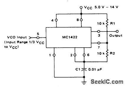
The VCO circuit, which has a nonlinear transfer characteristic, will operate satisfac-torily up to 200 kHz. The VCO input range is effective from1/3 VCC to VCC - 2 V, with the highest control voltage producing the lowest output frequency. (View)
View full Circuit Diagram | Comments | Reading(229)
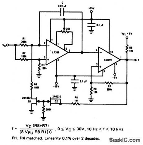
PRECISION_VOLTAGE_CONTROLLED_OSCILLATOR
Published:2009/7/1 20:58:00 Author:May
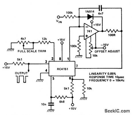
RC 4151 precision voltage-to-frequency converter generates a pulse train output linearly proportional to the input voltage. (View)
View full Circuit Diagram | Comments | Reading(2495)
10_Hz_TO_10_kHz_VOLTAGE_CONTROLLED_OSCILLATOR
Published:2009/7/1 20:47:00 Author:May
View full Circuit Diagram | Comments | Reading(836)
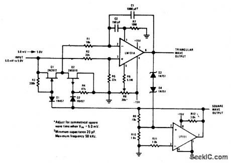
LINEAR_VOLTAGE_CONTROLLED_OSCILLATOR
Published:2009/7/1 20:46:00 Author:May
The linearity of input sweepvoltage versusoutput frequency is significantlyimproved by using an op amp. (View)
View full Circuit Diagram | Comments | Reading(0)
ASTABLE_OSCILLATOR
Published:2009/7/1 19:56:00 Author:May
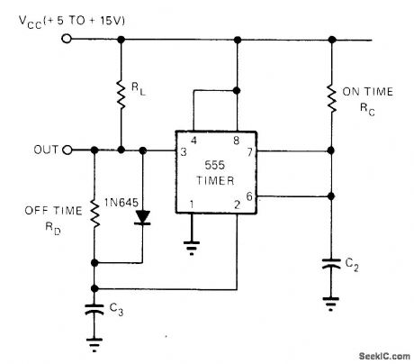
Circuit for astable operation of 555 timer provides completely independent ON and OFF times. Time constant for one mode is 1.1 RCC2 and for other mode is 1.1 RCC3. Free-running period is sum of these time constants.-J. P. Carter, Astable Operation of IC Timers Can Be lmproved, EDN Magazine, June 20, 1973, p 83. (View)
View full Circuit Diagram | Comments | Reading(0)
CRYSTAL_STABILIZED_IC_TIMER_CANPROVIDE_SUBHARMONIC_FREQUENCIES
Published:2009/7/1 3:59:00 Author:May

View full Circuit Diagram | Comments | Reading(641)
CRYSTAL_CONTROLLED_OSCLLATOR_OPERATES_FROM_ONE_MERCURY_CELL
Published:2009/7/1 3:51:00 Author:May
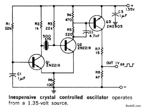
The circuit is powered by a single 1.35 V mercury cell and provides a 1 V squarewave output. As shown, the crystal is a tuned circuit between transistors Q1 and Q2, which are connected in the common-emitter configuration. Positive feedback provided by means of R permits oscillation. The signal at the collector of Q2 is squared by Q3, which switches between cutoff and saturation. R7 permits short-circuit-proof operation. (View)
View full Circuit Diagram | Comments | Reading(972)
HIGH_FREQUENCY_CRYSTAL_OSCILLATOR
Published:2009/7/1 3:48:00 Author:May
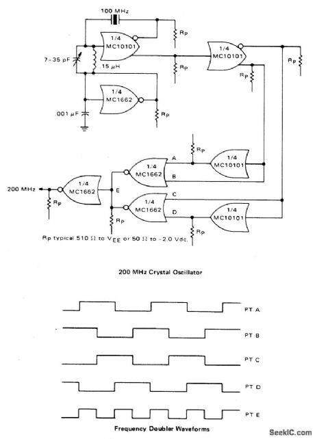
A high speed oscillator is possible by combining an MECL 10 K crystal oscillator with an MECL III frequency doubler as shown. One section of the MC10101 is connected as a 100 MHz crystal oscillator with the crystal in series with the feedback loop. The LC tank circuit tunes the 100 MHz harmonic of the crystal and may be used to calibrate the circuit to the exact frequency. A second section of the MC10101 buffers the crystal oscillator and gives complementary 100 MHz signals. The frequency doubler consists of two MC10101 gates as phase shifters and two MC1662 NOR gates. For a 50% duty cycle at the output, the delay to the true and complement 100 MHz signals should be 90°. This may be built precisely with 2.5 ns delay lines for the 200 MHz output or approximated by the two MC10101 gates. The gates are easier to incorporate and cause only a slight skew in output signal duty cycle. The MC1662 gates combine the 4 phase 100 MHz signals as shown in Figure B. The outputs of the MC1662's are wire-OR connected to give the 200 MHz signal. MECL III gates are used because of the bandwidth required for 200 MHz signals. One of the remaining MC1662 gates is used as a Vgg bias generator for the oscillator. By connecting the NOR output to the input, the circuit stays in the center of the logic swing or at VBB. A 0.001 μF capacitor ensures the VBB circuit does not oscillate. (View)
View full Circuit Diagram | Comments | Reading(0)
CRYSTAL_CONTROLLED_OSCILLATOR
Published:2009/7/1 3:43:00 Author:May
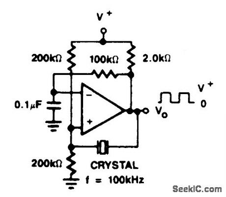
View full Circuit Diagram | Comments | Reading(0)
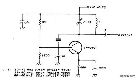
COLPITTS_OSCILLATOR
Published:2009/7/1 3:42:00 Author:May
Bias for the pnp bipolar transistor is provided by resistor voltage divider network R1/R2. The collector of the oscillator transistor is kept at ac ground by capacitor C5, placed close to the transistor. Feedback is provided by capacitor voltage divider C2/C3. (View)
View full Circuit Diagram | Comments | Reading(0)
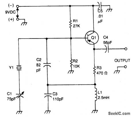
OVERTONE_CRYSTAL_OSCILLATOR
Published:2009/7/1 3:40:00 Author:May
This oscillator is designed for overtone crystals in the 20-100 MHz range operating in the third and fifth mode. Operating frequency is determined by the tuned circuit. (View)
View full Circuit Diagram | Comments | Reading(0)
| Pages:39/54 At 202122232425262728293031323334353637383940Under 20 |
Circuit Categories
power supply circuit
Amplifier Circuit
Basic Circuit
LED and Light Circuit
Sensor Circuit
Signal Processing
Electrical Equipment Circuit
Control Circuit
Remote Control Circuit
A/D-D/A Converter Circuit
Audio Circuit
Measuring and Test Circuit
Communication Circuit
Computer-Related Circuit
555 Circuit
Automotive Circuit
Repairing Circuit