
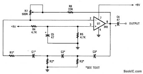
Oscillator Circuit
Index 28
SUPER_LOW_DISTORTION_VARIABLE_SINE_WAVE_OSCILLATOR
Published:2009/7/10 1:35:00 Author:May
View full Circuit Diagram | Comments | Reading(841)
SINGLE_SUPPLY_WIEN_BRIDGE_OSCILLATOR
Published:2009/7/10 1:33:00 Author:May
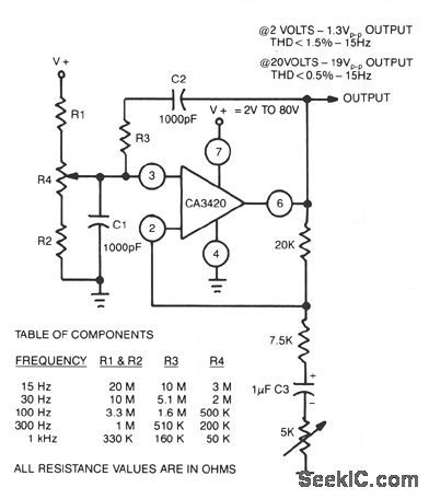
The adjustment of R4 contributes to the comparatively symmetrical output transfer characteristic of the CA3420 BiMOS op amp. To extend the lower operating frequency, remove C3 and use a dual supply. (View)
View full Circuit Diagram | Comments | Reading(1026)
LOW_DISTORTION_THERMALLY_STABILIZED_WIEN_BRIDGE_OSCILLATOR
Published:2009/7/10 1:32:00 Author:May
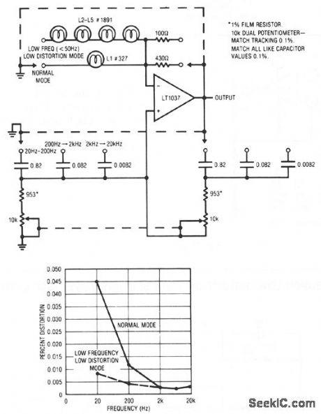
A variable Wien bridge provides frequency tuning from 20 Hz to 20 kHz. Gain control comes from the positive temperature coefficient of the lamp. When power is applied, the lamp is at a low resistance value, the gain is high, and oscillation amplitude builds. The lamp's gain-regulating behavior is flat within 0.25 dB over the 20 Hz-20 kHz range of the circuit. Distortion is below 0.003%. At low frequencies, the thermal time constant of the small normal-mode lamp begins to introduce distortion levels about 0.01%. This is because of hunting when the oscillator's frequency approaches the lamp's thermal time constant. This effect can be eliminated, at the expense of reduced output amplitude and longer amplitude settling time, by switching to the low-frequency, low-distortion mode. The four large lamps give a longer thermal time constant, and distortion is reduced. (View)
View full Circuit Diagram | Comments | Reading(835)
SINE_AND_SQUARE_WAVE_TTL_OSCILLATOR
Published:2009/7/10 1:32:00 Author:May
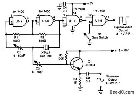
Using a Quad NAND Gate, the TTL oscillator can use fundamental crystals between 1 and 10 MHz. The sine-wave output is taken directly from the crystal, which acts as its ovrn filter, and yields a fairly clean sine wave. Adjust C1 and C2 for the best sine wave and also to set the crystal frequency. TTL square wave can be taken from U1D. The gate switch can be replaced with a Iogic gate to electronically control the output. (View)
View full Circuit Diagram | Comments | Reading(7029)
WIEN_BRIDGE_OSCILLATOR_1
Published:2009/7/10 1:29:00 Author:May
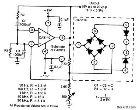
This circuit makes excellent use of high input impedance, high slew rate, ties of CA3140 BiMOS op amp, in combination with CA3019 diode array. (View)
View full Circuit Diagram | Comments | Reading(0)
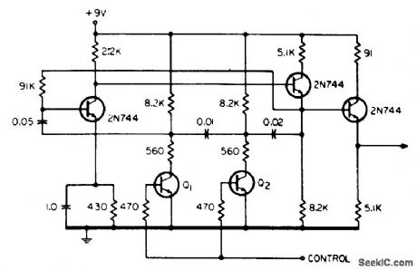
WIEN_BRIDGE_OSCILLATOR
Published:2009/7/10 1:28:00 Author:May
This complex oscillator circuit uses a photocell and common-mode-suppression circuitry to achievedistortion of 0.0003%。 (View)
View full Circuit Diagram | Comments | Reading(0)
THREE_DECADE_15_Hz_TO_15_kHz_WIEN_BRIDGE_OSCILLATOR
Published:2009/7/10 1:26:00 Author:May
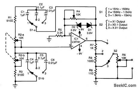
In this circuit, an LM741 op amp drives a Wien-bridge network using two zener diodes as an ampli-tude limiter. Range selection is done 'oy switch selecting the capacitors (C1 through C6) and tuning is done via a ganged pot. The output is about 8 Vpp max., depending on the setting of S2 and R6. R4 is set for maximum distortion consistent with stable output. (View)
View full Circuit Diagram | Comments | Reading(1784)
LOW_FREQUENCY_LO_OSCILLATOR
Published:2009/7/10 1:25:00 Author:May
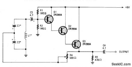
Basically a Hartley oscillator using a triple-emitter follower, this oscillator can be used at audio and low radio frequencies. The frequency is given by:At 1 kHz, typically C would be 4.7 μF tantalums, but this is only a guide as to convenient values to use. (View)
View full Circuit Diagram | Comments | Reading(987)
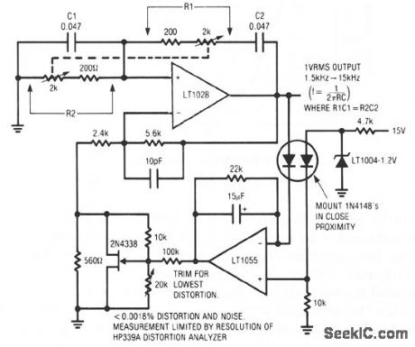
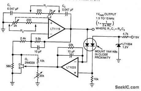
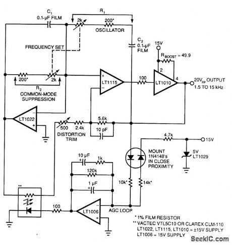
VERY_LOW_DISTORTION_OSCILLATOR
Published:2009/7/10 1:24:00 Author:May
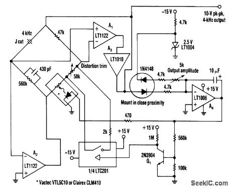
his oscillator uses a bridge circuit with an optoisolator as a gain-control device. The resultant distor-tion can be held to 9 ppm (.0009%) with proper adjustment. (View)
View full Circuit Diagram | Comments | Reading(827)
WIEN_BRIDGE_BASED_OSCILLATOR_WITH_VERY_LOW_DISTORTION
Published:2009/7/10 1:20:00 Author:May
This complex oscillator circuit uses a photocell and common-mode-suppression circuitry to achieve distortion of 0.0003%. This oscillator circuit replaces the lamp in the traditional Wien bridge with an elec-tronic equivalent. (View)
View full Circuit Diagram | Comments | Reading(1049)
500_MC_COLPITTS
Published:2009/7/19 23:41:00 Author:Jessie
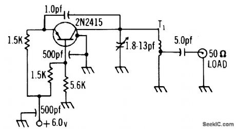
Frequency varies less than 3 Mc from 25 to 75℃, and less than 1.5 Mc with bias change from 6 to 9 V. Output is 10 mw. T1 is 1.5 length of 3/8 brass rod with output tap 1/4 from bottom.-Texas Instruments Inc., Solid-State Communications, McGraw-Hill, N.Y., 1966, p 301. (View)
View full Circuit Diagram | Comments | Reading(781)
TEMPERATURE_STABLE_200_MC
Published:2009/7/19 23:40:00 Author:Jessie
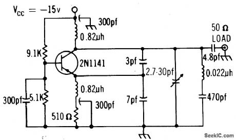
Varies less than 2 Mc in frequency and less than 1.5 mw in power output over temperature range of 25 to 80℃. Normal power output is 22.5 mw. -Texas Instruments Inc., Solid-State Communications, McGraw-Hill, N.Y., 1966, p 301. (View)
View full Circuit Diagram | Comments | Reading(793)
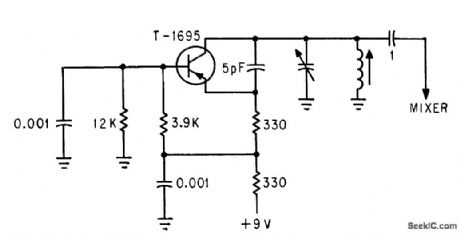
TWO_TRANSISTOR_SINE_WAVE_OSCILLATOR
Published:2009/7/10 1:07:00 Author:May
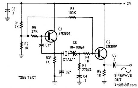
This oscillator uses two transistors and operates the crystal in the fundamental mode. C1 and C2 should be about 2 700 pF for 1 MHz, 680 pF for 5 MHz, and 330 pF for 10 MHz. 150 pF can be used for up to 20 MHz. The output is a near perfect sine wave. Try varying C1 and C2 for best waveform. About 2 to 6 Vpp is available. (View)
View full Circuit Diagram | Comments | Reading(2728)
NONLINEAR_VOLTAGE_CONTROLLED_OSCILLATOR
Published:2009/7/19 23:39:00 Author:Jessie
Use of conventional transistors rather than fet's means that Q1 and Q2 operate in knee region, where frequency does not vary linearly with d-c control voltage. This is generally not a drawback when control voltage is servoed. Increasing the control voltage increases the frequency.-R. Selleck, Voltage-Controlled Oscillators, EEE, 13:3, p 47. (View)
View full Circuit Diagram | Comments | Reading(805)
BRIDGED_T_R_C_PHASE_SHIFT_OSCILLATOR
Published:2009/7/19 23:37:00 Author:Jessie
Emitter-follower eliminates loading variations, contributing to exceptional frequency stability (0.2%) over temperature range of -55 to 80℃.- Transistor Manual, Seventh Edition, General Electric Co., 1964, p 207. (View)
View full Circuit Diagram | Comments | Reading(755)
STABLE_40_MC_OSCILLATOR
Published:2009/7/19 23:36:00 Author:Jessie
Frequency shifts less than 500 kc when supply voltage is changed from 5 to 12 V.-T. P. Prouty, Using Varactors to Extend Frequency-Control Range, Electronics, 36:45, p 48-49. (View)
View full Circuit Diagram | Comments | Reading(763)
VARICAP_TUNES_TUNNEL_DIODE_OSCILLATOR
Published:2009/7/19 23:35:00 Author:Jessie
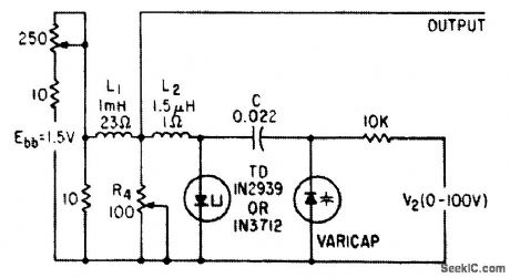
Series oscillator circuit tunes electrically over range of 12 to 22 Mc.-E. Gottlieb and J. Giorgis, Tunnel Diodes-Using Them as Sinusoidal Generators, Electronics, 36:24, p 36-42. (View)
View full Circuit Diagram | Comments | Reading(1914)
DAMPED_40_MC_GENERATOR
Published:2009/7/19 23:34:00 Author:Jessie
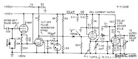
Converts unit pulses, resulting from video screening in nuclear track scanner, to damped 40-Mc oscillations each 0.1 microsec long, which are inserted in quartz ultrasonic delay line that feeds counter.-P. V. C. Hough, J. A Koenig, and W. Williams, Scanner Recognizes Atomic Particle Tracks, Electronics, 32:13, p 58-61. (View)
View full Circuit Diagram | Comments | Reading(810)
BALANCED_TMO_VCO
Published:2009/7/10 0:23:00 Author:May
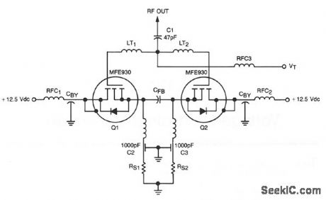
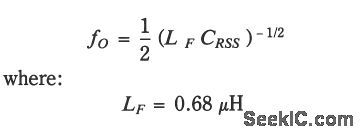
This TMOS VCO operates in push-pull to produce 4 W at 70 MHz. It consists of two MFE930 TMOS devices in a balanced VCO that generally provide better linearity than the single-ended types. Varactors are not used because the design takes advantage of the large change in Miller capacitance, CRSS, that is available in TMOS gate structures.In the balanced VCO, the fundamental (fo) and/or twice the fundamental (2fo) can be coupled from the circuit at separate nodes. This makes the balanced oscillator very useful in phase-locked loops. The fundamental: (View)
View full Circuit Diagram | Comments | Reading(717)
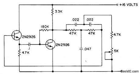
VARYING_FREQUENCY_OSCILLATOR
Published:2009/7/9 23:29:00 Author:May
Output frequency of alarm tone generator changes continuously. With suitable ampliler and loudspeaker, can easily be heard in noisy environments where single tone or amplitudemodulated tone would go unnoticed.-A. Jnall, Varying-Frequency Warning Alarm, EEE, l2:7, p 25. (View)
View full Circuit Diagram | Comments | Reading(792)
| Pages:28/54 At 202122232425262728293031323334353637383940Under 20 |
Circuit Categories
power supply circuit
Amplifier Circuit
Basic Circuit
LED and Light Circuit
Sensor Circuit
Signal Processing
Electrical Equipment Circuit
Control Circuit
Remote Control Circuit
A/D-D/A Converter Circuit
Audio Circuit
Measuring and Test Circuit
Communication Circuit
Computer-Related Circuit
555 Circuit
Automotive Circuit
Repairing Circuit