
Oscillator Circuit
Index 33
OSCILLATOR_FOR_CHANNELS_2_6
Published:2009/7/7 20:56:00 Author:May
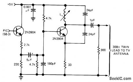
Transmitter serving as interface between video game and TV set can be tuned with L1 to vacant chan, nol in low TV band. Regular antenna should be disconnected when output of oscillator is fed to TV set via twin-line, to avoid broadcasting game signals. L1 is 4tums No. 18 spaced 3/8 inch on 1/4-inch slug-tuned form.-B. Matteson, King Pong Game Offers Hockey and Tennis Alternatives to TV Re-Runs, EDN Magazine, Aug. 5, 1975, p 47-55. (View)
View full Circuit Diagram | Comments | Reading(855)
50_MHZ_VHF_CRYSTAL_OSCILLATOR
Published:2009/7/7 7:57:00 Author:May
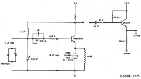
Figure 21-14 shows a 50-MHz oscillator operating on a third harmonic. The collector's load resistor R1 has been increased because the quartz crystal's internal series resistance RS increases with frequency in the VHF range. The crystal's internal series resistance RS is 3Ω , and the transistor's minimum current gain HFE is 100. Using the same technique as for the 20 MHz oscillator, the external series RLCL equivalent load seen by the 50 MHz crystal is 5.6Ω (RL) and 1000 pF (CL). (View)
View full Circuit Diagram | Comments | Reading(1095)
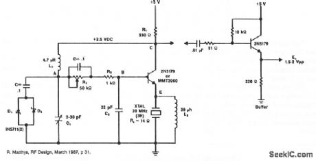
100_MHz_VHF_CRYSTAL_OSCILLATOR
Published:2009/7/7 7:53:00 Author:May

Figure 21-13 shows a 100-MHz oscillator operating on the fifth harmonic. Again to maintain the transistor's gain, note the increase in the collector's load resistance R1 because of the increase in the quartz crystal's internal series resistance Rs. C3 is needed at frequencies above 50 MHz to tune out the shunting effect of L1 on R1, to maintain a high load resistance for the transistor and get enough gain for oscillation.The equivalent series RLCL load across the crystal is 8.2 Ω (RL) and 200 pF (CL).
(View)
View full Circuit Diagram | Comments | Reading(2023)
20_MHz_VHF_CRYSTAL_OSCILLATOR
Published:2009/7/7 7:47:00 Author:May
A typical circuit at 20 MHz is shown. The crystal, which has an internal series resistance RS, of 14 Ω , oscillates at its third harmonic. The diode clamp D1 and D2 provides a constant amplitude control. The transistor operates continuously in a linear mode over a complete cycle of oscillation, and reflects a reasonably constant load across the crystal at an times. (View)
View full Circuit Diagram | Comments | Reading(816)
TEMPERATURE_COMPENSATED_CRYSTAL_OSCILLATOR
Published:2009/7/7 7:27:00 Author:May
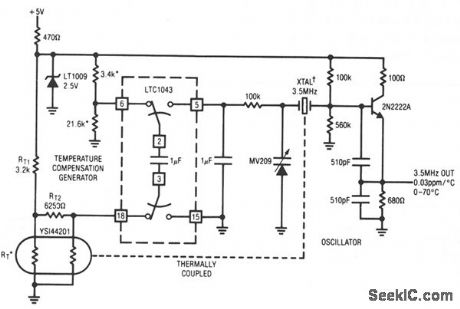
This circuit uses LTC1043 to differentiate between a temperature sensing network and a dc reference. The single-ended output biases a varactor-tuned crystal oscillator to compensate drift. The varactor crystal network has high dc impedance, eliminating the need for an LTC1043 output amplifier.
(View)
View full Circuit Diagram | Comments | Reading(0)
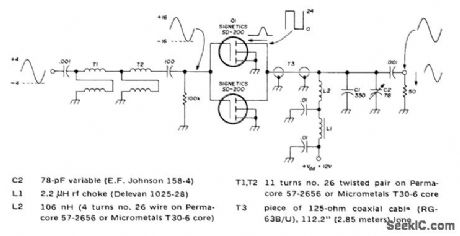
CRYSTAL_CONTROLLED_REFLECTION_OSCILLATOR
Published:2009/7/7 7:25:00 Author:May
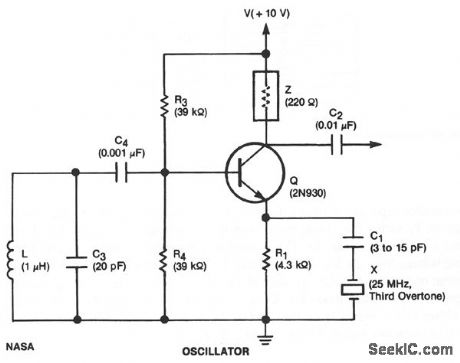
This unit is easily tunable and stable, consumes little power, and costs less than other types of oscillators that operate at the same frequencies. This unusual combination of features is made possible by a design concept that includes operation of the transistor well beyond the 3 dB frequency of its current-versus-frequency curve. The concept takes advantage of newly available crystals that resonate at frequencies up to about 1 GHz.
The emitter of transistor Q is connected with variable capacitor C1 and series-resonant crystal X.The emitter is also connected to ground through bias resistor R1. The base is connected to the parallel combination of inductor L and capacitor C3 through dc-blocking capacitor and C4 and is forward biased with respect to the emitter by resistors R3 and R4. Impedance Z could be the 220-Ω resistor shown or any small impedance that enables the extraction of the output signal through coupling capacitor C2. If Z is a tuned circuit, it is tuned to the frequency of the crystal. (View)
View full Circuit Diagram | Comments | Reading(899)
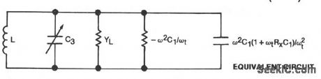
TWO_GATE_QUARTZ_OSCILLATOR
Published:2009/7/7 7:18:00 Author:May
A SN7400 quartz crystal and a resistor provide a square-wave output of approximately 3.5 V. The circuit operates reliably at frequencies from 120 kHz to 4 MHz. (View)
View full Circuit Diagram | Comments | Reading(2475)
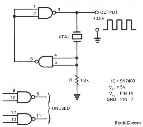
VOLTAGE_CONTROLLED_CRYSTAL_OSCILLATOR
Published:2009/7/7 7:16:00 Author:May
A voltage-variable capacitance tuning diode is placed in series with the crystal feedback path. Changing the voltage on VR varies the tuning diode capacitance and tunes the oscillator. The 510-KΩ resistor, R1, establishes a reference voltage for VR-ground is used'm this example. A 100-KΩ resistor, R2, isolates the tuning voltage from the feedback loop and 0.1-μF capacitor C2 provides ac coupling to the tuning diode. The circuit operates over a tuning range of 0 to 25 V. It is possible to change the tuning range from 0 to 25 V by reversing the tuning diode Dl. Center frequency is set with the 2 -60 pf trimmer capacitor.Deviation on either side of center is a function of the crystal frequency. The table in Fig. 21-7 shows mea-sured deviation in parts per million for several tested crystals. (View)
View full Circuit Diagram | Comments | Reading(1865)
LOW_FREQUENCY_PIERCE_OSCILLATOR
Published:2009/7/7 7:14:00 Author:May
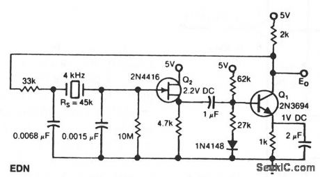
The Pierce circuit oscillates at 4 kHz.At low frequencies,the crystal's internal senes resistance RS isquite high (45 K at 4 kHz).Therefore,all FET-based source follower is included to prevent Q1 from loading the crystal output. (View)
View full Circuit Diagram | Comments | Reading(1051)
SIMPLE_CMOS_CRYSTAL_OSCILLATOR
Published:2009/7/7 7:10:00 Author:May
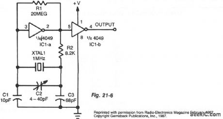
The circuit is an inverter set up as a linear amplifier. Adding the crystal and capacitors to the feedback path, we tum the amplifier into an oscillator and force it to oscillate at, or least very near, the crystal's resonant frequency. Trimmer capacitor C2 adjusts the actual operating frequency of the circuit. The crystal should be a parallel-resonant type; maximum frequency will depend partly on supply voltage, but it should be possible to go to at least 1 MHz. (View)
View full Circuit Diagram | Comments | Reading(2286)
1_MHz_PIERCE_OSCILLATORS
Published:2009/7/7 7:09:00 Author:May
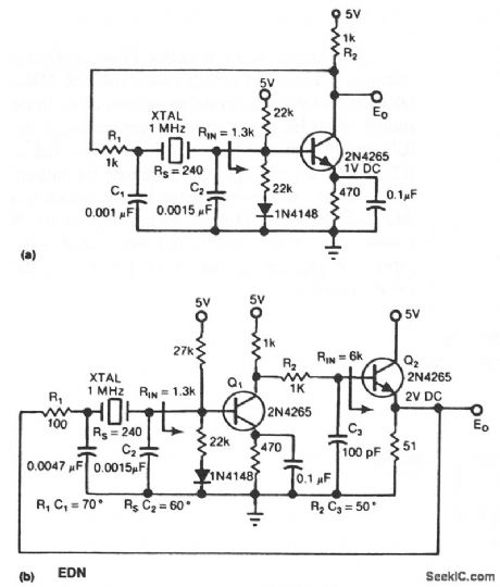
Simple network design is a key feature of the Pierce circuit, as these 1-MHz oscillators illustrate .Operating the crystal slightly above resonance (Fig.21-5a) requires only one high-gain transistor stage.Operating it exactly at series resonance (Fig. 21-5b) requires an extra RC phase lag and two transistors which can have lower gain. (View)
View full Circuit Diagram | Comments | Reading(2565)
EASY_START_UP_CRYSTAL_OSCILLATOR
Published:2009/7/7 7:06:00 Author:May
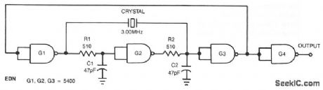

This low cost, crystal-controlled oscillator uses one TTL gate. Two factors ensure oscillator start-up: The connection of NAND gates G1, G2, and G3 into an unstable logic configuration and the high loop gain of the three inverters. Values of R1, R2, C1, and C2 aren't critical; select them so the oscillator operates at a frequency 70 to 90% higher than the crystal frequency when the crystal is disconnected. For 1-2 MHz operation, a low-power 54L00IC is recommended; for a 2-6 MHz, a standard 5400 type; and for 6-20 MHz, a 54H00 or 54S00.
(View)
View full Circuit Diagram | Comments | Reading(897)
FUNDAMENTAL_FR_EQUENCY_CRYSTAL_OSCILLATOR_2_60_PF_Qopendingon_Frquoncy_FREQUENCY_RANGE__1_0_N
Published:2009/7/7 7:04:00 Author:May
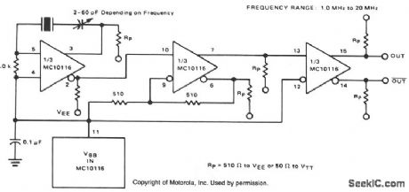
For frequencies below 20 MHz, a fundamental-frequency crystal can be used and the resonant tank is no longer required. Also, at this lower frequency range the typical MECL 10,000 propagation delay of 2 ns becomes small compared to the period of oscillation, and it becomes necessary to use a noninverting output. Thus, the MC10116 oscillator section functions simply as an amplifier. The 1.0 KΩ resistor biases the line receiver near VBBand the 0.1-μF capacitor is a filter capacitor for the VBB supply. The capacitor, in series with the crystal, provides for minor frequency adjustments. The second section of the MC10116 is connected as a Schmitt-trigger circuit; this ensures good MECL edges from a rather slow, less than 20-MHz input signal. The third stage of the MC10116 is used as a buffer and to give complementary outputs from the crystal oscillator circuit. The circuit has a maximum operating frequency of approximately 20 MHz and a minimum of approximately 1 MHz; it is intended for use with a crystal which operates in the fundamental mode of oscillation. (View)
View full Circuit Diagram | Comments | Reading(1490)
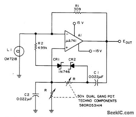
EASILY_TUNED_SINE_WAVE_SQUARE_WAVE_OSCILLATOR
Published:2009/7/7 6:18:00 Author:May
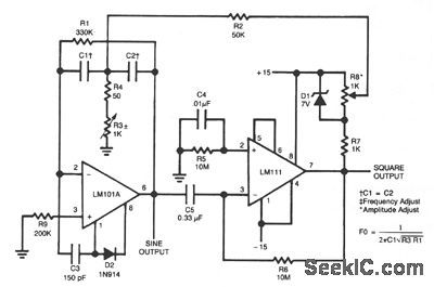
The circuit will provide both a sine- and square-wave output for frequencies from below 20 Hz to above 20 kHz. The frequency of oscillation is easily tuned by varying a single resistor. This is a considerable advantage over Wien-Bridge circuits where two elements must be tuned simultaneously to change frequency. Also, the output amplitude is relatively stable when the frequency is changed. An amp is used as a tuned circuit, driven by square wave from a voltage comparator. The frequency is controlled by R1, R2, C1, C2, and R3, with R3 used for tuning. Tuning the filter does not affect its gain or bandwidth, so the output amplitude does not change with frequency.A comparator is fed with the sine-wave output to obtain a square wave. The square wave is then fed back to the input of the tuned circuit to cause oscillation. Zener diode, D1, stabilizes the amplitude of the square wave fed back to the filter input. Starting is insured by R6 and C5 which provide dc negative feed-back around the comparator. This keeps the comparator in the active region. Distortion ranges between 0.75% and 2% depending on the setting of R3. Although greater tuning range can be accomplished by increasing the size of R3 beyond 1 KΩ, distortion becomes excessive. Decreasing R3 lower than 50 Ω can make the filter oscillate by itself. (View)
View full Circuit Diagram | Comments | Reading(939)
20_METER_VFO
Published:2009/7/7 4:26:00 Author:May
Tunes from 14.0 to 14.2 MHz、using stable Vackar design, Protective diode CR1 canbe any silicon rectifier Clamping diode CR3 improves stability by preventing conduction in gate of JFET osciliator Q1,-C,E,Galbreath、Low-Power Solid-State VFO Transmit-ter for 20 Meters,Ham Radio. Nov,1973, p 6-11 (View)
View full Circuit Diagram | Comments | Reading(1206)
SQUARE_TRIANGLE_VCO
Published:2009/7/6 23:42:00 Author:May
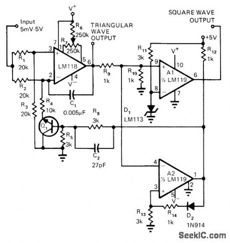
With DC control voltage of 5 mV to 5 V, circuit controls frequency of both square and triangle outputs with good linearity. Peak value of triangle output is precisely set at 2.44 V and 0 V by reference voltages at noninverting inputs of comparators.Comparator A2 drives load for low outputs, while comparator A1 drives load when output is high. Article tells how circuit works.-R. C.Dobkin, Comparators Can Do More Than Just Compare, EDN Magazine, Nov. 1, 1972, p 34-37. (View)
View full Circuit Diagram | Comments | Reading(1175)
ADJUSTABLE_SINE_WAVE_AUDIO_OSCILLATOR
Published:2009/7/6 22:01:00 Author:May
Circuit Notes
Waveform purity at low frequencies for a Wien bridge oscillator is enhanced by diode limiting. Lamp L1 stabilizes the loop gain at higher frequencies while the limiting action of R2, CR1, and CR2 prevents clipping at low frequencies and increases the frequency adjustment range from about 3:1 to greater than 10:1. (View)
View full Circuit Diagram | Comments | Reading(711)
A_555_USED_AS_AN_RC_AUDIO_OSCILLATOR
Published:2009/7/6 21:57:00 Author:May
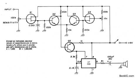


Circuit Notes
Transistor Q5 and the 1000 ohm resistor form the variable element needed for controlling the frequency of VDO by limiting the charging current flowing into the 0.15μF timing capacitor according to the forward bias being applied to Q5. As the voltage on pins 2 and 6 of U1 reach 2/3 VCC (about 6 volts with a 9-volt supply) the timer will fire and pin 3 will be pulled low. Pin 7, an open collector output, goes low and begins to discharge the timing capacitor-through the 3.3 kilohm resistor. The discharge time provided by this resistor assures a reasonable, although asymmetrical, waveform for the aural signal generated by U1. At 1/3 VCC the intemal flip-flop resets, the output on pin 3 goes high, the open collector output on pin 7 floats, and the timing cycle begins again. (View)
View full Circuit Diagram | Comments | Reading(1038)
LOW_COST_WIEN_BRIDGE_OSCILLATOR
Published:2009/7/6 21:51:00 Author:May
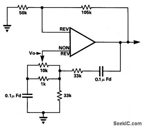

Circuit Notes
In the circuit the frequency trimming component is arranged so that the voltage across it is in quadrature with the voltage V, from the bridge so that as it is adjusted the attenuation of the bridge only changes a little, avoiding the need for a two gang component. The range of variation of frequency is very limited. By using a high gain amplifier and metal film feedback resistors the loop gain can be set so that the unit just oscillates and the use of an automatic gain setting component, a thermistor for example, is eliminated. (View)
View full Circuit Diagram | Comments | Reading(1283)
CALIBRATING_MARK_SPACE_VCO
Published:2009/7/6 21:32:00 Author:May
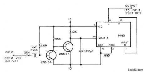
Simple buffer/counter provides accurate calibration of FSK circuit used in cassette interface of 8080 microprocessor to generate mark and space frequencies. Audio FSK waveform is squared and divided down in 7493 4-bit counter. Resulting pulses are fed to input port of microprocessor for software pulse counting. Software sets VCO frequency, waits until pulse starts, counts each pulse occurrence, and displays resultant count.Each 7493 count is 29 Hz or 14.5μs, so 371 counts correspond to 2975 Hz for space. Mark frequency of 2125 Hz gives pulses separated by 519 counts.-D. R. Bourdeau, Cassette Interface First Aid, Kilobaud, July 1977, p 49. (View)
View full Circuit Diagram | Comments | Reading(1595)
| Pages:33/54 At 202122232425262728293031323334353637383940Under 20 |
Circuit Categories
power supply circuit
Amplifier Circuit
Basic Circuit
LED and Light Circuit
Sensor Circuit
Signal Processing
Electrical Equipment Circuit
Control Circuit
Remote Control Circuit
A/D-D/A Converter Circuit
Audio Circuit
Measuring and Test Circuit
Communication Circuit
Computer-Related Circuit
555 Circuit
Automotive Circuit
Repairing Circuit