
Audio Circuit
Index 23
Strain_gauge_with_thermoelectric_junction_effects
Published:2009/7/22 3:41:00 Author:Jessie
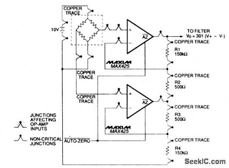
This circuit shows the previous strain-gauge example (Fig. 1-11) with low-level nodes highlighted and shown as thermoelectric junctions. An even number of connections cancels the errors as long as no temperature gradients appear across the circuit. Such gradients are best prevented by symmetric PC layouts with traces sized for matched thermal conductivity. In extreme cases, the circuitry can also be insulated from external heat sources and drafts. (View)
View full Circuit Diagram | Comments | Reading(936)
Strain_gauge_amplifier
Published:2009/7/22 3:37:00 Author:Jessie
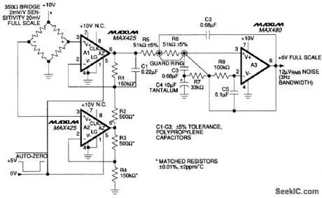
In the circuit, two MAX425s (A1 and A2) amplify the differential 20-mV full-scale output of a strain-gauge bridge. The signal is then filtered and buffered by a MAX480 (A3). The 3-Hz bandwidth of the filter limits output noise to about 12 μVrms (40 nVrms referred to the input). This translates to a signal-to-noise ratio of 114dB, which allows stable measurements to within a few parts per million. (View)
View full Circuit Diagram | Comments | Reading(3493)
AUDIO_SQUELCH
Published:2009/7/22 1:21:00 Author:Jessie
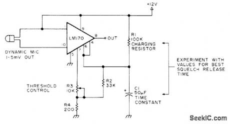
Used to suppress back-ground noise during intervals between sentences and words when operating amateur radio station on VOX and using compressor. Circuit attenuates audio path below preset input level determined by setting of R3.-Circuits, 73 Magazine, May 1977, p 19. (View)
View full Circuit Diagram | Comments | Reading(2301)
Dc_and_bridge_titles_and_descriptions
Published:2009/7/22 2:12:00 Author:Jessie
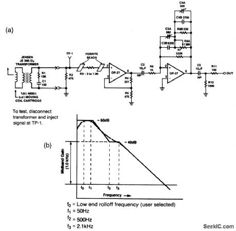
The circuit of Fig. 1-1A is adjusted to match a 40-dB RIAA curve (Fig.1-1B). With break points at 50, 500, and 2100 Hz, the entire curve is fixed by a specified gain at1 kHz. The circuit is designed for use with newer moving-coil magnetic phono cartridges, which have a sensitivity of 0.1 mV per CM/S (compared to older cartridges with sensitivities of1 mV per CM/S). The circuit is adjusted by injecting a low-level signal into TP-1, with the transformer disconnected. At 100 Hz, adjust C3A for an output level that is 6 dB lower than the low-frequency output. At 1000 Hz, adjust R8A for an output level 20 dB lower than the low-frequency output. At 21 kHz, adjust C4A for an output that is 40 dB less than the low-frequency output. Raytheon Linear integrated Circuits 1989, p 4-78, 4-79. (View)
View full Circuit Diagram | Comments | Reading(891)
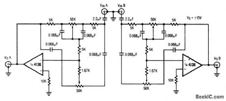
RIAA_preamplifier
Published:2009/7/22 2:23:00 Author:Jessie
This circuit also uses only one half of the 4136 (Fig.1-4). (View)
View full Circuit Diagram | Comments | Reading(0)
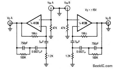
Stereo_tone_control
Published:2009/7/22 2:22:00 Author:Jessie
This circuit uses only one-half of the 4136(Fig.l-5) (View)
View full Circuit Diagram | Comments | Reading(0)
Compressor_expander_amplifiers
Published:2009/7/22 2:19:00 Author:Jessie
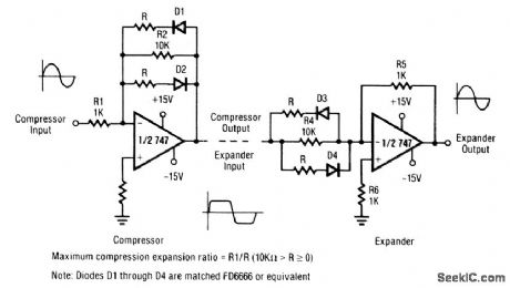
The maximum compression/expansion ratio of these circuits is set by the ratio of R1/R,as shown. (View)
View full Circuit Diagram | Comments | Reading(2617)
Low_impedance_microphone_Preamplifier
Published:2009/7/22 2:17:00 Author:Jessie
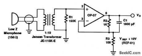
The low microphone impedance is matched to the OP-37 by thetransformer.C1 rolls off the high-frequency response at 90 kHz,giving a noise power bandwidth of 140 kHz. The REF-01 voltage reference is described In Fig.4-1. (View)
View full Circuit Diagram | Comments | Reading(0)
Low_noise_and_drift_FET_dc_amplifier
Published:2009/7/22 3:35:00 Author:Jessie
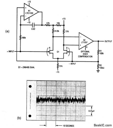
This circuit combines the low drift or a chopper-stabilized amplifier with a pair of FETs. As shown in Fig. 1-10B, the result is an amplifier with 0.05-μV/℃ drift, offset within 5 μV, 50-pA bias current, and 200-nV noise in a 0.1-to 10-Hz bandwidth. (View)
View full Circuit Diagram | Comments | Reading(1081)
Low_noise_and_drift_dc_amplifier
Published:2009/7/22 3:32:00 Author:Jessie
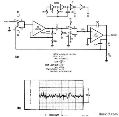
This circuit combines the low noise of an LT1028 with a chopper-based carrier-modulation scheme to get a very low-noise, low-drift dc amplifier. As shown in Fig. 1-9B, noise in a 0.1- to 1-Hz bandwidth is less than 40 nV with 0.05 μV/℃ drift. In general, to maintain this low-noise performance, the source resistance should be kept below 500Ω. Such resistance is typical of transducers (strain-gauge bridges, magnetic detectors, etc.). (View)
View full Circuit Diagram | Comments | Reading(1634)
Switchable_audio_amplifier
Published:2009/7/22 3:27:00 Author:Jessie
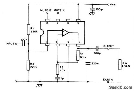
The SL6310 shown in this figure is a low-power audio amplifier that can be switched off by applying a mute signal to pins 7 or 8. Despite the low quiescent current consumption of 5 mA (only 0. 6 mA when muted), a minimum output power of400 mW is available into an 8-Ω load from a 9-V supply. With the values shown, the voltage gain is about 25, determined by the ratio of (R3+R4)/R3, with an input impedance of about 100KΩ), determined by,R1 and R2. (View)
View full Circuit Diagram | Comments | Reading(1092)
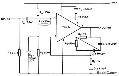
Gain_controlled_microphone_preamplifier_VOGAD
Published:2009/7/22 3:25:00 Author:Jessie
The SL6270 shown in this figure combines the functions of audio amplifier and voice-operated gain-adjusting device (VOGAD). The SL6270 accepts signals from a low-sensitivitymicrophone and provides an essentially constant output signal for a 50-dB range of input. Thedynamic range, attack time, and decay time are controlled by external components. With thevalues shown. attack time(time taken for the output to return to within 10% of the original level following a 20-dB increase in input level)is about 20mS.decay rate is 20 dB/s .voltagegain is 52 dB with 72μVrms input at pin4,output level=90mVrms with 4mVrms input at pin4,and an input impedance of 150Ω. (View)
View full Circuit Diagram | Comments | Reading(3243)
Magnetic_cartridge_preamplifier
Published:2009/7/22 3:23:00 Author:Jessie
This circuit provides an approximate gain of 50 (34 dB) at 1 kHz with a distortion of 0.004%. If more gain is required, R3 can be decreased, but C3 must be increased proportionally to avoid loss of bias. C1, C2, R1, R2 provide RIAA equalization. C3 and R3 provide a rumble filter. The S/N ratio is better than 70 dB below a 5-mV input. (View)
View full Circuit Diagram | Comments | Reading(979)
Constant_voltage_crossover_network
Published:2009/7/23 21:11:00 Author:Jessie
This active crossover network provides 12-dB/octave slopes, where the crossover frequency is determined by: 1/(6.28RC). Figure 1-46B shows both the low-pass and high-pass responses, with a crossover frequency of 1kHz. Notice that the summed response (dashed lines) is perfectly flat. (View)
View full Circuit Diagram | Comments | Reading(1588)
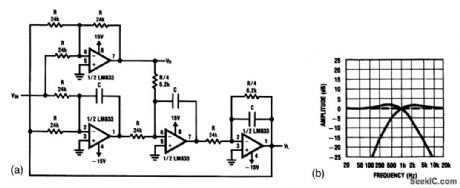
Low_cost_high_level_preamp_and_tone_control
Published:2009/7/22 20:19:00 Author:Jessie
This circuit uses the JFET to best advantage (low impedance). All device parameters are non-critical, yet the circuit achieves harmonic distortion of less than 0.05% with a S/N ratio of over 85 dB. The tone controls allow 18-dB of cut and boost. The amplifier has a 1-V output for 100-mV input at maximum level. (View)
View full Circuit Diagram | Comments | Reading(1453)
Discrete_component_audio_amplifier_7_to_35_W_pnp_driver
Published:2009/7/22 4:11:00 Author:Jessie
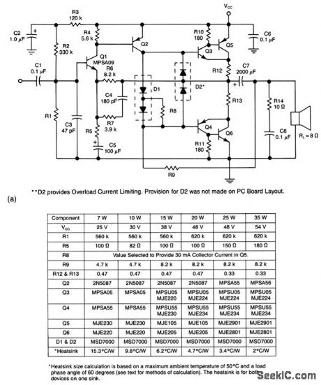
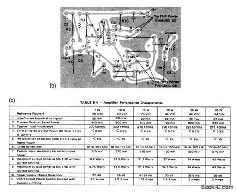
This circuit provides a 1- to 35-W output, depending on power source and component values (as shown), with overload protection. Figures 1-19B and 1-19C show the PC-board layout and performance characteristics, respectively. (View)
View full Circuit Diagram | Comments | Reading(1278)
TONE_RINGER_Ⅱ
Published:2009/7/6 20:47:00 Author:May
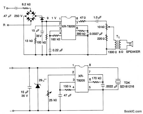
The XR-T8205 Tone Ringer is primarily intended as a replacement for the mechanical telephone bell. The device can be powered directly from telephone ac ringing voltage or from a separate dc supply. An adjustable trigger level is provided with an external resistor. The circuit is designed for nominal 15 volt operation.
(View)
View full Circuit Diagram | Comments | Reading(1168)
Ratiometric_bridge_with_A_D_conversion
Published:2009/7/22 3:50:00 Author:Jessie
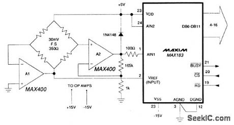
In this circuit, a MAX183 directly converts a bridge output to a 12-bit code using only two precision op amps. No differential-input instrumentation amplifier or reference is needed. The bottom of the bridge is driven by A1 so that the A1 inverting input remains at 0 V. The other bridge output is amplified by A2 in a basic noninverting configuration. No differential amplifier is needed because the bridge output to A2 is referenced to 0 V. The A1 output also drives the MAX183 VREF input so that reference changes (VDD is the reference) in the bridge excitation and the A/D track each other. (View)
View full Circuit Diagram | Comments | Reading(976)
TONE_RINGER
Published:2009/7/6 20:45:00 Author:May
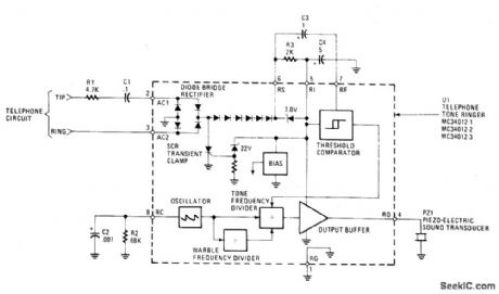
The MC34012 tone-ringer chip derives its power by rectifying the ac ringing signal.That signal is normally at 20 Hz and measures between 70 and 130 volts rms. It uses that power for the tone generator and to drive the piezoelectric transducer. The sound that is produced is a warble that varies between two frequencies, f0/4 (f0 - 4) f0/5.The clock, or fundamental, frequency, f0, is generated by a relaxation oscillator. That oscillator has R2 and C2 as its frequency setting components providing a selectable range of 1 kHz to 10 kHz. Selecting different values for R2 and/or C2 changes the clock frequency, which in turn varies the warble frequencies. The MC34012 chip comes in three different warble rates at which the warble frequencies (f0/4, f0/5) are varied. These warble rates are f0/320, f0/640, or f0/160 and the different chips are designated as MC34012-1, -2, and -3, respectively. For example: with a 4.40 kHz oscillator frequency, the MC34012-1 produces 800 Hz and 1000 Hz tones with a 12.5 Hz warble rate. The MC34012-2 generates 1600 Hz and 2000 Hz tones with a similar 12.5 Hz warble frequency from an 8.0 kHz oscillator frequency. MC34012-3 will produce 400 Hz and 500 Hz tones with a 12.5 warble rate from a 2.0 kHz oscillator frequency. (View)
View full Circuit Diagram | Comments | Reading(1080)
CARRIER_CURRENT_AUDIO_TRANSMITTER
Published:2009/7/6 20:40:00 Author:May
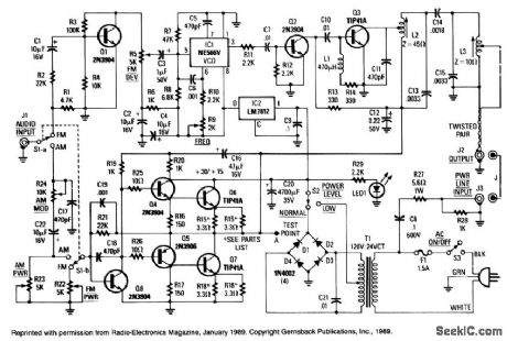
The decision to use either AM, narrowband FM (less than 15 kHz), or wideband FM (greater than 30 kHz) depends on the application. For the transmission of music, FM is better because it has greater noise immunity. For speech or other noncritical applications, AM may be satisfactory. Our transmitter permits either mode by switch selection.
Audio is fed from S1a to either the FM or AM circuitry. Starting with the FM section, amplifier Q1 accepts an audio signal in the 10 Hz to 20 kHz range of about 0.5 V peak-to-peak. The audio gain is adjusted via R5 to provide up to 60 kHz deviation of voltage-controlled oscillator IC1 which is set to nominally 280 kHz. IC1 and Q1 are supplied with a regulated 12 V from IC2. A square-wave signal from IC11pin 3 drives Q2, and Q2 drives the output amplifier Q3. A coupling network is used to match the nominal 45- Ω output impedance of Q3 to the 10- Ω ac line impedance.
In the AM mode, audio is coupled to Q8 via R24 and then amplified again by transistors Q4 to Q7. The normally stable dc voltage at test point A is thereby varied at an audio rate. Because Q2 and Q3 obtain their dc VCC from test point A, the VCO carrier input to Q2 is amplitude modulated by the varying VCC amplitude. That produces an amplitude-modulated output from the transmitter. Careful setting of carrier level R23 and audio level R24 provides up to 100% modulation. The kit is available from North Country Radio, P.O. Box 53, Wykagyl Station, NY 10804. (View)
View full Circuit Diagram | Comments | Reading(1448)
| Pages:23/54 At 202122232425262728293031323334353637383940Under 20 |
Circuit Categories
power supply circuit
Amplifier Circuit
Basic Circuit
LED and Light Circuit
Sensor Circuit
Signal Processing
Electrical Equipment Circuit
Control Circuit
Remote Control Circuit
A/D-D/A Converter Circuit
Audio Circuit
Measuring and Test Circuit
Communication Circuit
Computer-Related Circuit
555 Circuit
Automotive Circuit
Repairing Circuit