
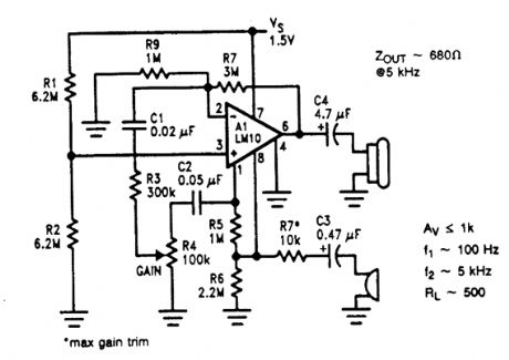
Audio Circuit
Index 32
MINI_MEGAPHONE
Published:2009/6/19 2:02:00 Author:May
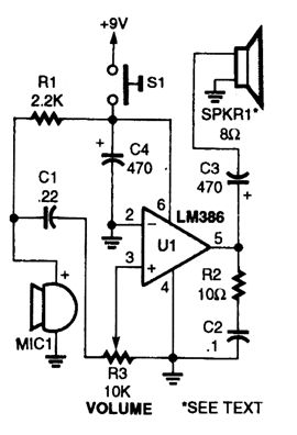
The Mini-Megaphone is comprised of an elec-tret microphone (MIC1), and LM386 low-voltage audio-power amplifier (U1), a horn speaker (SPKR1), and a few other components. (View)
View full Circuit Diagram | Comments | Reading(6)
AUDIO_EXPANDER
Published:2009/6/19 1:50:00 Author:May
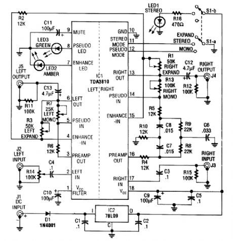
This audio processor is based on the Signetics/Philips TDA3810N stereo, spatial, pseudo-stereo processor, IC. This processor uses a Philips TDA3810IC device, and it functions as an expander, pseudo stereo processor, and audio enhancer. Pseudo stereo is obtained by routing various frequencies to each channel via active filters (View)
View full Circuit Diagram | Comments | Reading(6929)
HIGH_IMPEDANCE_MICROPHONE_INPUT_CIRCUIT
Published:2009/6/18 23:56:00 Author:May
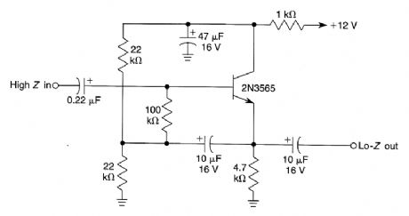
This input circuit will enable use of a high-impedance microphone where a low-impedance microphone would be needed. (View)
View full Circuit Diagram | Comments | Reading(1420)
SINGLE_ENDED_HI_Z_MICROPHONE_PREAMP
Published:2009/6/18 23:47:00 Author:May
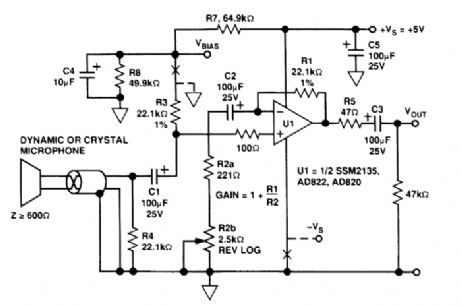
This low noise circuit works on a +5-V supply. Gain range is 20 to 40 dB and bandwidth is 20 kHz with the AD820. THD is 0.05% with 1 V RMS into a 2-kΩ load. Noise output with the input shorted is less than 200μV. (View)
View full Circuit Diagram | Comments | Reading(1474)
BALANCED_MICROPHONE_PREAMPLIFIER
Published:2009/6/18 23:44:00 Author:May
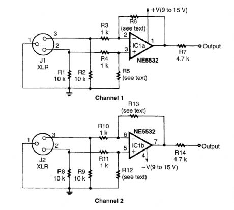
A balanced input for microphones can solve hum and noise pickup problems. R6 and R13 should equal R5 and R12, respectively. Typical values would be 10 kΩ to 22 kΩ. (View)
View full Circuit Diagram | Comments | Reading(8063)
DYNAMIC_MICROPHONE_PREAMP
Published:2009/6/18 23:43:00 Author:May
This preamplifier provides 40- to 43-dB gain when used with a low-impedance (<1kΩ) dynamic microphone (View)
View full Circuit Diagram | Comments | Reading(3)
10_NOTE_SOUND_SYNTHESIZER
Published:2009/6/18 22:52:00 Author:May
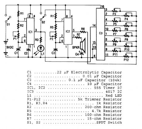
As shown, three ICs are used to produce the sounds. IC1 is a 555 timer that generates clock pulses. It is configured as an astable multivibrator. The frequency of the clock pulses is set by trim-mer potentiometer Pl. These clock pulses are coupled to the input of IC3 (a 4017 CMOS Johnson counter) on its clock input pin 14. Each clock pulse causes IC3 to shift a high to each of its output pins in sequence. A trimmer resistor, which can be adjusted to set a different frequency for each note, is connected to each of 103's output pins. One side of each of the trimmers is connected to pin 5 (the control voltage pin) of IC2.IC2, another 555 timer IC, creates the tone; the overall pitch of the tone can be varied by P2. As the output sequences from the 4017, that tone, which is changed in frequency by each output shift is applied to a srrtall speaker from pin 3 of IC2. An LED, which flashes with each clock pulse, is con-nected to pin 3 of IC1. Switch S2 is used to vary the sound between flowing and distinct notes. (View)
View full Circuit Diagram | Comments | Reading(1214)
TONE_CHIME
Published:2009/6/18 22:50:00 Author:May
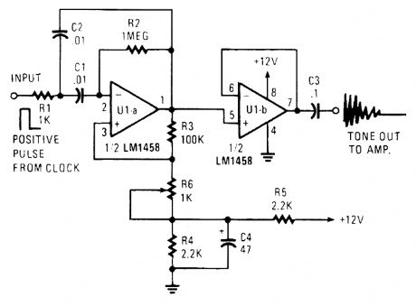
A positive pulse input to RI causes the active filter UI-a to ring. If the gain is set too high (R6), the circuit will oscillate. R6 controls the positive feedback and the Q of the circuit. C1 and C2 can be changed to adjust the tone frequency. (View)
View full Circuit Diagram | Comments | Reading(1146)
110_dB_BEEPER
Published:2009/6/18 22:45:00 Author:May
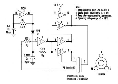
This circuit will gqnerate an ear-splitting 110 dB from 9 V. The setup uses a single 74C14 (CD40106B) CMOS hex inverting Schmitt-trigger IC, which must be used with a piezoelectric device with a feedback terminal. The feedback terminal is attached to a central region on the piezoelectric wafer. When the beeper is driven at resonance, the feedback signal peaks.One inverter of the 74C14 is wired as an astable oscillator. The frequency is chosen to be 5 times lower than the 3.2 kHz resonant frequency of the piezoelectric device. Feedback from the third pin of the beeper reinforces the correct drive frequency to ensure maximum sound output.Four other inverter sections of the IC are wired to form two separate drivers. The output of one section is cross-wired to the input of the second section. The differential drive signal that results produces about 18-V p-p when measured across the beeper. The last inverter section is wired as a second astable oscillator with a frequency of about 2 Hz. It gates the main oscillator on and off through a diode. For a continuous tone, the modulation circuit can be deleted. (View)
View full Circuit Diagram | Comments | Reading(1990)
CANARY_SOUND_SIMULATOR
Published:2009/6/18 22:42:00 Author:May
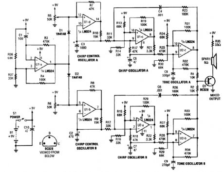
This circuit generates the sound of two canaries singing in a cage. Two LM324 quad amps make up seven oscillators. One os-cillator is an on/off control, the other six generate the sounds of two canaries. A 9-V supply powers the circuit. (View)
View full Circuit Diagram | Comments | Reading(1764)
LOW_VOLTAGE_MICROPHONE_PREAMP
Published:2009/6/18 22:41:00 Author:May
A microphone amplifier is shown. The refer-ence, with a 500-kHz unity-gain bandwidth, is used as a preamplifier with a gain of 100. Its out-put is fed through a gain-control potentiometer to the op amp, which is connected for a gain of 10. The combination gives a 60-dB gain with a 10-kHz bandwidth, unloaded, and 5 kHz loaded at 500Ω. Input impedance is 10 kΩ.Potentially, using the reference as a preampli-fier in this fashion can cause excess noise. How-ever, because the reference voltage is low, the noise contribution, which adds root-mean-square, is likewise low. The input noise voltage in this con-nection is 440-500 nV Hz, about equal to that of the op amp. (View)
View full Circuit Diagram | Comments | Reading(1119)
PTT_CONTROL_FROM_RECEIVER_AUDIO
Published:2009/6/18 2:51:00 Author:May
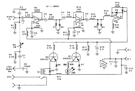
This system will key a transmitter or other device that can be keyed by a relay closure. Audio is amplified, limited, and is rectified and drives relay driver Q2 and LED indicator. The transmitter au-dio output was used to feed a keyed transmitter and can be deleted or ignored where this feature is unnecessary. (View)
View full Circuit Diagram | Comments | Reading(1640)
WIDEBAND_PREAMP
Published:2009/6/18 2:19:00 Author:May
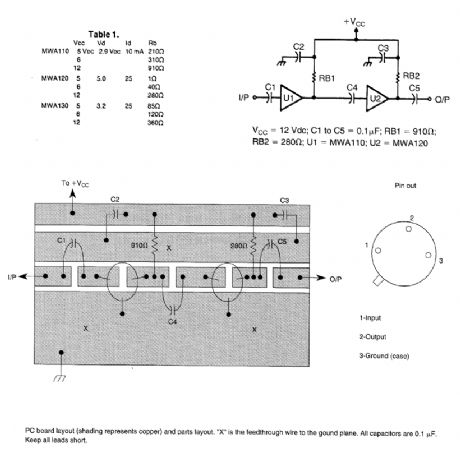
Motorola MWA 110,120,Or 130 are wideband amplifier ICs. This wideband preamp circuit can be used in many applications Keep the leads short when constructing the circuitry. (View)
View full Circuit Diagram | Comments | Reading(2123)
RECEIVER_SCANNER_PREAMP_USING_MAR_1_MMIC
Published:2009/6/18 1:50:00 Author:May
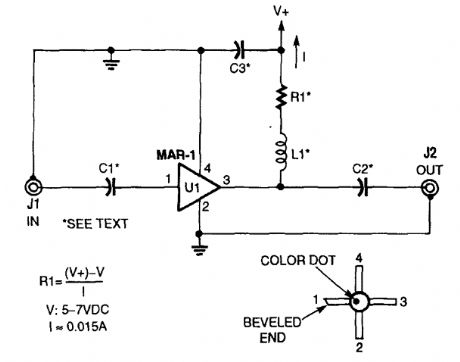
The low-cost Mini-Circuits MAR-X series of chips offer the RF builder a real advantage, with their inherent 50-Ω input and output impedances (needed for RF systems). An MAR-l-based re-ceiver/scanner preamplifier is shown. C1 and C2 are chip capacitors. Use 0.01 μF for HF, 0.001 for VHF, and 100 pF for above 100 MHz, depending on the low-frequency limit that you desire. C3 can be a ceramic disc of 0.01 μF or 0.001 μF, de-pending on frequency range. L1 is an RF choke that is suitable for the frequency range that you desire (0.1 to 10 μH). (View)
View full Circuit Diagram | Comments | Reading(2592)
HF_PREAMPLIFIER
Published:2009/6/17 23:15:00 Author:May
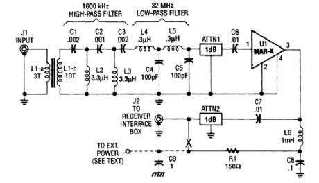
This HP SW receiver preamplifier is comprised of a broadband toroidal transformer (L1-a and L1-b), a complex LC network (comprised of a 1600-kHz, high-pass filter and a 32-MHz, low-pass fil-ter), L2 and L3 (26 turns of #26 enameled wire wound on an Amidon Associates T-50-2, red, toroidal core), a pair of resistive attenuators (ATTN1 and ATTN2), and of course, the MAR-x device. Exter-nal power for the preamp can be 9 to 12 Vdc. R1 can be increased in value for higher voltages. (View)
View full Circuit Diagram | Comments | Reading(1380)
AGC_AUDIO_PREAMP
Published:2009/6/17 22:52:00 Author:May
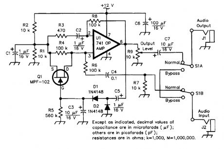


The circuit uses an easily obtained 741 op amp set for an internal gain of about 200. A portion of the op amp's output signal is rectified by the 1N4148 diodes, then filtered and fed to the gate of the FET input shunting circuit. As the output rises, more and more input shunting takes place. That is, more of the input signal is bypassed, effectively keeping the output level constant.The circuit offers a 100:1 limiting action. The input level can change over a 100:1 ratio with little or no effect on the output level. The output level itself can be set from less than unity all the way up to nearly the gain of the amplifier, making the circuit usable in other applications as well. (View)
View full Circuit Diagram | Comments | Reading(5540)
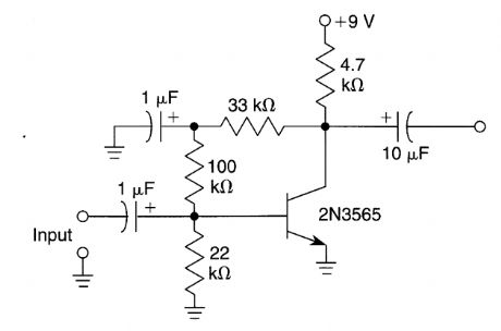
SELECTIVE_PREAMPLIFIER_FOR_INFRARED_PHOTODIODE
Published:2009/6/16 22:15:00 Author:May
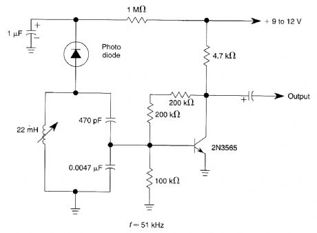
The circuit uses a tuned circuit to achieve frequency selection. Values are for operation at about 51 kHz. The 2N3565 amplifies the output developed by the tuned circuit. (View)
View full Circuit Diagram | Comments | Reading(1204)
DUAL_PREAMP
Published:2009/6/15 23:06:00 Author:May

If you wish to amplify low-levle signals,such as the output of a turntable, the signal must first be fed to this preamp. (View)
View full Circuit Diagram | Comments | Reading(1118)
LOOP_ANTENNA_PREAMPLIFIER
Published:2009/6/15 21:16:00 Author:May

This preamplifier has a built-in regeneration control boost gain selectivity. C1 is a single or multigang AM broadcast-band tuning capacitor. L1 is a ferrite loop antenna, tapped at about 15 to 25% of total turns. This circuit should prove useful for low-frequency (up to 3 MHz) reception, where a loop would be advantageous to reduce man-made noise pickup. (View)
View full Circuit Diagram | Comments | Reading(4485)
HF_BROADBAND_ANTENNA_PREAMP
Published:2009/6/15 21:06:00 Author:May

The HP/SW receiver preamplifier is comprised of a broadband toroidal transformer (L1-a and L1-b), LC network (corrtprised of a 1600-kHz, high-pass filter and a 32-MHz, low-pass filter), L2 and L3 (26 turns of #26 enameled wire wound on an Amidon Associates 7-50-2, red, toroidal core), a pair of resistive attenuators (ATTN1 and ATTN2), and a MAR-x device.Shown here is the composition of a basic 1-dB pi-network resistor antenuator. This is the method of supplying dc power to a preamplifier using only the RE coax cable. (View)
View full Circuit Diagram | Comments | Reading(2054)
| Pages:32/54 At 202122232425262728293031323334353637383940Under 20 |
Circuit Categories
power supply circuit
Amplifier Circuit
Basic Circuit
LED and Light Circuit
Sensor Circuit
Signal Processing
Electrical Equipment Circuit
Control Circuit
Remote Control Circuit
A/D-D/A Converter Circuit
Audio Circuit
Measuring and Test Circuit
Communication Circuit
Computer-Related Circuit
555 Circuit
Automotive Circuit
Repairing Circuit