
Audio Circuit
Index 22
PAL_NTSC_DECODER_WITH_RGB_INPUTS
Published:2009/7/9 2:14:00 Author:May
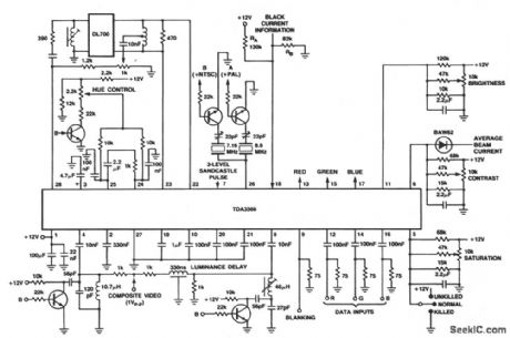
This circuit shows the TDA3566 for a PAL/NTSC Decoder. (View)
View full Circuit Diagram | Comments | Reading(2648)
AUDIO_DITHERIZING_CIRCUIT_FOR_DIGITAL_AUDIO_USE
Published:2009/7/9 1:47:00 Author:May
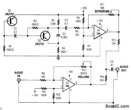
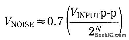
By adding a small amount of noise to a signal to be digitized (about 0.7 bit):
where: n=# of bits. For example, 8 bits and 2 V p-p would be 0.0055 V.
This circuit uses a transistor (Q1) and an amplifier (Q2 and U1) to generate controls the noise signal,R11 controls the noise injection and R12 controls the gain of the system. (View)
View full Circuit Diagram | Comments | Reading(985)
DARKROOM_ENLARGER_TIMER
Published:2009/7/9 1:41:00 Author:May
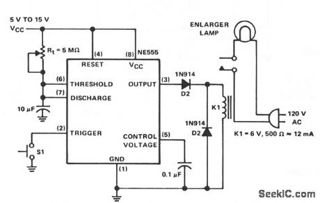
The NE555 circuit is a basic one-shot timer with a relay connected between the output and ground. It is triggered with the normally open momentary contact switch, which when operated, grounds the trigger input at pin 2. This causes a high output to energize K1 which closes the normally open contacts in the lamp circuit. They remain closed during the timing interval, then open at time out. Timing is controlled by a 5-MΩ potentiometer, Rt. All timerdriven relay circuits should use a reverse clamping diode, such as D1, across the coil. The purpose of diode D2 is to prevent a timer output latch-up condition in the presence of reverse spikes across the relay.With the rc time constant shown, the full-scale time is about 1 minute. A scale for the 5-MΩ potenti-ometer shaft position can be made and calibrated in seconds. Longer or shorter full-scale times can be achieved by changing the values of the rc timing components. (View)
View full Circuit Diagram | Comments | Reading(1495)
AUDIO_EQUALZER
Published:2009/7/8 23:58:00 Author:May
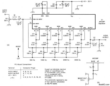
Designed for communications use, this equalizer circuit uses a Mitsubishi M5226P audio equalizer IC to adjust frequency response. It runs from a 9 to 20 V supply. C6 through C16 are polyester film capacitors of ± 5% tolerance. (View)
View full Circuit Diagram | Comments | Reading(5215)
AUDIO_FADER
Published:2009/7/8 23:55:00 Author:May
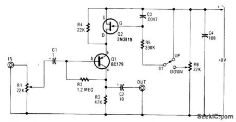
In this circuit, Q1 is a simple amplifier that has its gain controlled by a variable emitter resistance supplied by FET Q2. In the up position of S1, C3 discharges through R5 and the gain of Q1 decreases because Q2 is driven toward cut-off. In the down position, Q2 conducts more, depending on the setting of R6, which causes a gain increase. By varying R5 or C3, various fade rates can be obtained. (View)
View full Circuit Diagram | Comments | Reading(1662)
CRYSTAL_CONTROLLED_AUDIO_GENERATOR
Published:2009/7/21 2:06:00 Author:Jessie
In this circuit, two signals from crystal oscillators operating at nearly the same frequency are mixed in Q2 and the audio difference frequency is used. C3 is a small air padder capacitor of 3 to 40 pF and can be fitted with a dial that is calibrated in the audio frequency producedi C2 is used for an initial calibration of the fixed oscillator to exactly 10.000 MHz. (View)
View full Circuit Diagram | Comments | Reading(907)
TV_sound_channel_with_2_watt_output_using_an_ECG742
Published:2009/7/21 4:35:00 Author:Jessie
TV sound channel with 2-watt output using an ECG742. Supply voltage is from 18 to 27 volts. The chip is a 16-pin DiP. The circuitcan be connected toan 8-ohm load and still provide the 2-watt output (courtesy GTE Sylvania Incorporated). (View)
View full Circuit Diagram | Comments | Reading(978)
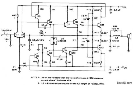
15__20__25__35__50__60_watt_AF_power_amplifier_with_AC_coupled_output
Published:2009/7/20 20:52:00 Author:Jessie
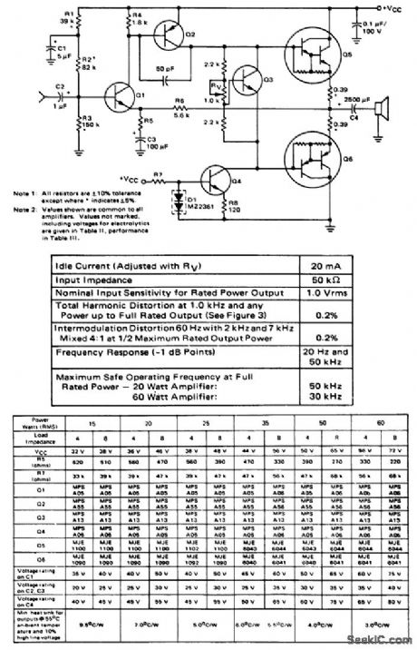
15-/20-/25-/35-/50-/60-watt AF power amplifier with AC-coupled output (courtesy Motorola Semiconductor Products Inc.). (View)
View full Circuit Diagram | Comments | Reading(1017)
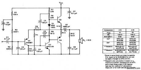
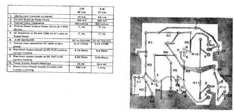
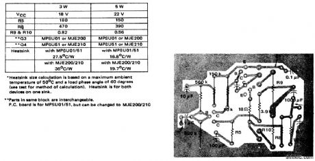
3_watt_5_watt_AF_power_amplifier_with_NPN_driver
Published:2009/7/20 21:18:00 Author:Jessie
3-watt/5-watt AF power amplifier with NPN driver (courtesy Motorola Semiconductor Products Inc.). (View)
View full Circuit Diagram | Comments | Reading(2061)
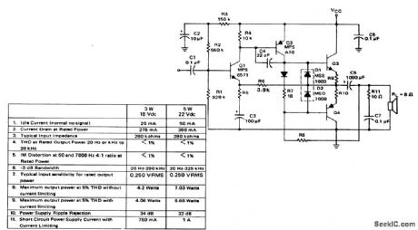
3_watt_5_watt_AF_power_amplifier_with_PNP_driver
Published:2009/7/20 21:13:00 Author:Jessie
3-watt/5-watt AF power amplifier with PNP driver (courtesy Motorola Semiconductor Products Inc.). (View)
View full Circuit Diagram | Comments | Reading(1022)
15__20__25_watt_AF_power_amplifier_with_Darlington_outputs
Published:2009/7/20 21:35:00 Author:Jessie
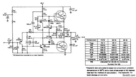
15-/20-/25-watt AF power amplifier with Darlington outputs (courtesy Motorola Semiconductor Products Inc.). (View)
View full Circuit Diagram | Comments | Reading(3598)
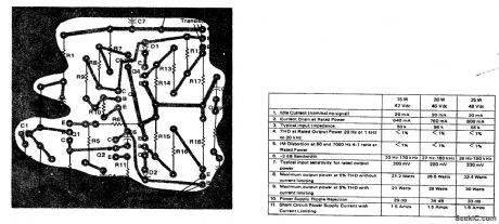
35__50__60__75__100_watt_AF_power_amplifier
Published:2009/7/20 21:45:00 Author:Jessie
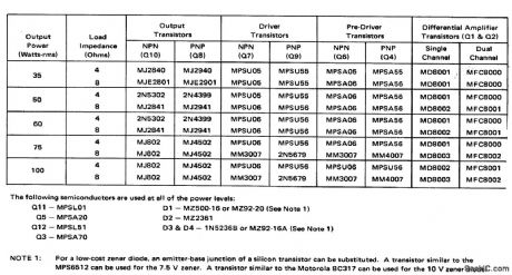
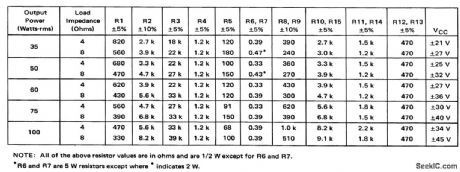
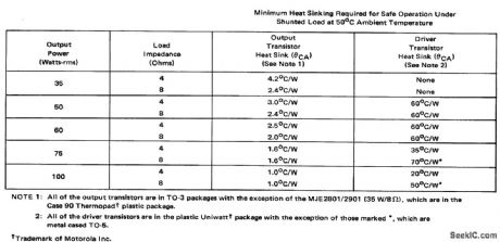
35-/50-/60-/75-/100-watt AF power amplifier (courtesy Motorola Semiconductor Products Inc.). (View)
View full Circuit Diagram | Comments | Reading(3173)
UNIVERSAL_MIXER_STAGE
Published:2009/7/8 4:30:00 Author:May
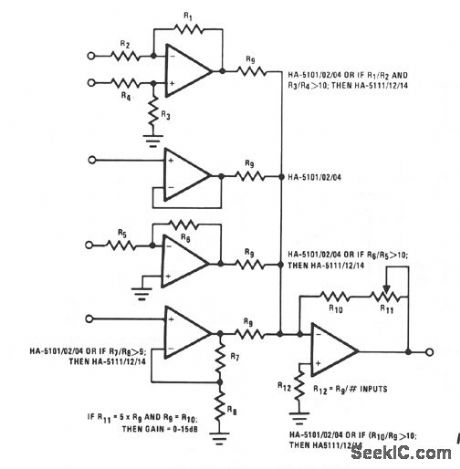
This circuit illustrates some possible buffer combinations. These include a differential input stage, a voltage follower as well as both noninverting and inverting stages. The allowable resistor ratios and recommended device types are also included. One restriction applies to this type of mixer network in which Rg is greater than 2.4 KΩ. This limits the worst case output current for each of the input buffers to less than 10 mA.
(View)
View full Circuit Diagram | Comments | Reading(1082)
FOUR_CHANNEL_MIXER
Published:2009/7/8 4:28:00 Author:May
View full Circuit Diagram | Comments | Reading(0)
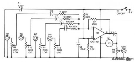
INPUT_BUFFERED_MIXER
Published:2009/7/8 4:27:00 Author:May
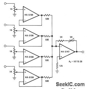
A high signal-to-noise ratio is important in stgnal construction and combination. The HA-5147 aids in lowering overall system noise and thereby raises system sensitivity. The signal combination circuit incorporates input buffering with several other features to form a relatively efficient mixer stage with a minimum of channel crosstalk. The potentiometer used for each channel allows for both variable input levels and a constant impedance for the driving source. The buffers serve mainly to prevent reverse crosstalk back through the resistor network. This buffering allows for the combination of varying strength signals without reverse contamination. The gain of the final stage is set at a minimum of 10 and can be adjusted to as much as 20.This allows a great amount of flexibility when combining a vast array of input signals. (View)
View full Circuit Diagram | Comments | Reading(1350)
SIMPLE_MIXER
Published:2009/7/8 4:26:00 Author:May
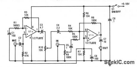
This mixer is built around a TL072 dual BiBET op anp with a JFET input stage,and can be powered from a single-ended 9-to 18-V power surry.The microphone input is capacitively coupled to the noninverting input of U1a.
Resistors R1 and R3 set the voltage gain at about 26 dB and serve as a negative feedback network for U1a.Capacitors C1 through C3 are dc-blocking capacitors.Most high-impedance microphones have outputs of a few mV.Often,a preamp stage just isn't enough,so the microphone signal is given a boost of about 20 db in the mixer.The noninverting input of U1b is biased to half the surry voltage by R6,R7,and C6.Rsistors R5 and R8 make up the negative-feedback network and set the voltage gain of U1b at unity.Capacitor C5 is for dc blocking at this input. (View)
View full Circuit Diagram | Comments | Reading(656)
ACID_RAIN_MONITOR
Published:2009/7/8 4:11:00 Author:May
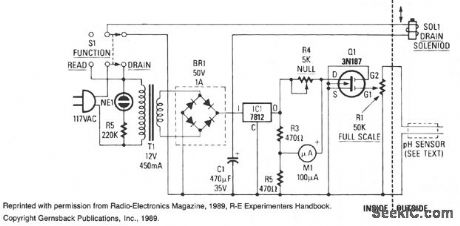
A simple bridge rectifier and a 12-V regulator powers the MOSFET sensing circuit. The unregulated output of the bridge rectifier operates the drain solenoid via switch S1. The sensor itself is built from two electrodes: one made of copper, the other of lead. In combination with the liquid trapped by the sensor, the electrodes form a miniature lead/acid cell whose output is amplifted by MOSFET Q1. The maximum output produced by our prototype cell was about 50 μA.MOSFET Q1 serves as the fourth leg of a Wheatstone bridge. When sensed acidity causes the sensor to generate a voltage, Q1 turns on slightly, so its drain-to-source resistance decreases. That resistance variation causes an imbalance in the bridge, and that imbalance is indicated by meter M1. (View)
View full Circuit Diagram | Comments | Reading(0)
BROADBAND_MIXER
Published:2009/7/7 23:36:00 Author:May
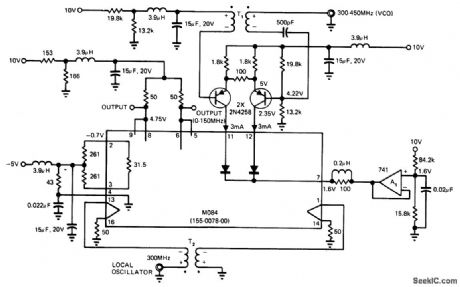
Uses Tektronix M084 multiplier as broadband mixer having linear output within -3 dB limit from 2 MHz to above150 MHz. Current-gain cell in multiplier takes advantage of logarithmic relationship between current and voltage in a semiconductor. Output function includes product of two Input signals,a300-450MHz swept VCO signal and a 300-MHz local oscillator signal.-M .Jaffe, Build a Low Cost Wideband Mixer with a Monolithic Multiplier, EDN Magazine. May 20,1975,p63-64. (View)
View full Circuit Diagram | Comments | Reading(1240)
PHONE_RECORDER
Published:2009/7/7 22:21:00 Author:May
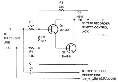
This recorder can be connected to the telephone lines just about any place, and no external power source is needed. The tape recorder's switch terminals are applied to a pair of transistors, connected as Darlingtons, that are used to turn the recorder on and off. When the telephone is off-hook there's usually about 50 Vdc across the phone that's divided over R1, R2, and R4, so that Q1's base is negative enough to keep the recorder off. Pick up the receiver, and the voltage drops to 5 V. That leaves not quite-enough voltage on Q1's base to keep that transistor at cutoff, so the recorder begins. Remember to keep your recorder's switch in the on position, and depending on how many people use the telephone, remember to rewind or change tapes occasionally! (View)
View full Circuit Diagram | Comments | Reading(1235)
Ultrasonic_receiver
Published:2009/7/22 3:43:00 Author:Jessie
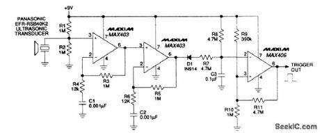
This low-power ultrasonic receiver, built around two MAX403s, can operate for several weeks on a 9-V battery. The receiver has high gain at ultrasonic frequencies to detect faint reflections from a separate ultrasonic source (not shown). To prevent false triggering, the 40-kHz received signal passes through R7 to charge C3 after being rectified by D1. The rectified signal is detected by a MAX406 op amp, connected as a comparator, chosen because of its 1-μA supply current and rail-to-rail output swing. (View)
View full Circuit Diagram | Comments | Reading(6)
| Pages:22/54 At 202122232425262728293031323334353637383940Under 20 |
Circuit Categories
power supply circuit
Amplifier Circuit
Basic Circuit
LED and Light Circuit
Sensor Circuit
Signal Processing
Electrical Equipment Circuit
Control Circuit
Remote Control Circuit
A/D-D/A Converter Circuit
Audio Circuit
Measuring and Test Circuit
Communication Circuit
Computer-Related Circuit
555 Circuit
Automotive Circuit
Repairing Circuit