
Audio Circuit
Index 33
WIDEBAND_ANTENNA_PREAMPLIFIER
Published:2009/6/15 21:02:00 Author:May
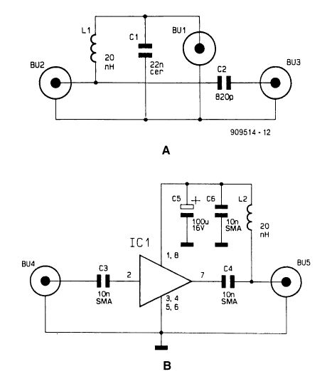
This wideband antenna preamplifier has a gain of around 20 dB from 40 to 860 MHz, covering the entire VHF, FM, commercial, and UHF bands. A phantom power supply provides dc to the preamp via the coaxial cable feeding the unit. (View)
View full Circuit Diagram | Comments | Reading(2517)
VLF_60_kHz_ANTENNA_PREAMP
Published:2009/6/15 20:57:00 Author:May
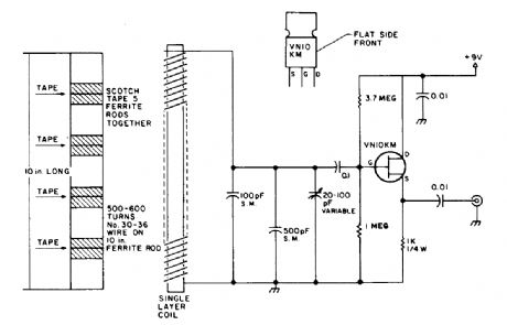
Suitable for 60-kHz standard frequency reception, here is a schematic for a FET preamp and antenna. (View)
View full Circuit Diagram | Comments | Reading(2744)
GENERAL_PURPOSE_PREAMPLIFIER
Published:2009/6/15 4:08:00 Author:May

Suitable for general audio use, the preamp circuit uses a feedback pair. Current gain is set by the ratio of (R4 + R6)/R4. (View)
View full Circuit Diagram | Comments | Reading(1)
AUDIO_TO_UHF_PREAMP
Published:2009/6/15 3:57:00 Author:May
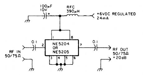
The Signetics NE5204 or NE5205 can be used in this AF to 350-MHz (-30 dB) preamp. If 600MHz @ 3dB is needed, use the NE5205. The noise figure is 4.8dB at 75Ω, 6dB at 50Ω. Gain is approximately +20dB over the passband. (View)
View full Circuit Diagram | Comments | Reading(1340)
FREQUENCY_COUNTER_PREAMP
Published:2009/6/15 3:56:00 Author:May
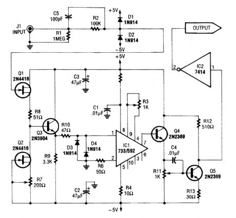
Based on the LM733 or NE592, the preamp shown has a bandwidth of 100 MHz. The FET inputs provide about 1-MΩ input impedance. Q4, Q5, and IC2 provide signal conditioning. (View)
View full Circuit Diagram | Comments | Reading(8)
GENERAL_PURPOSE_JFET_PREAMP
Published:2009/6/15 3:31:00 Author:May
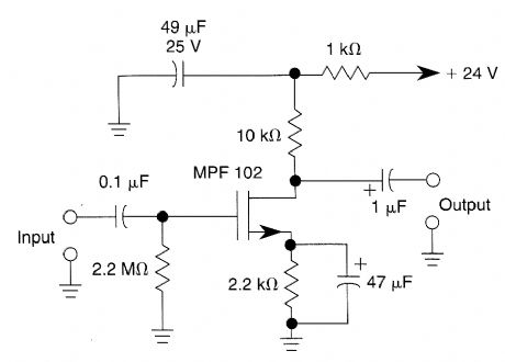
This JFET preamplifier has a gain of about 20dB and a bandwidth of over 100kHz. It is use-ful as a low-level audio amplifier for high-imped-ance sources. (View)
View full Circuit Diagram | Comments | Reading(1632)
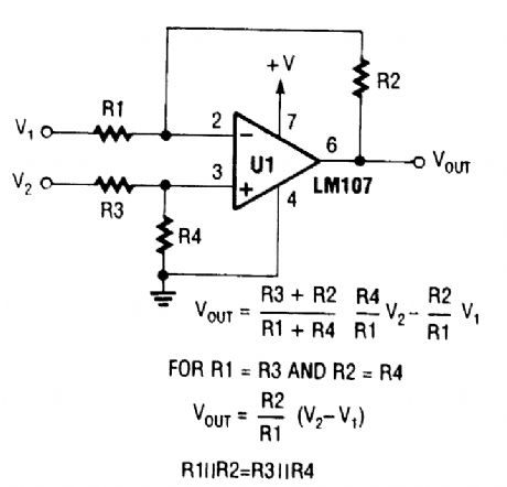
Balanced Output Circuit Composed of Double Operational Amplifier
Published:2011/7/18 2:55:00 Author:Sue | Keyword: Balanced, Output, Double, Operational Amplifier
The picture shows the balanced output circuit composed of double operational amplifier. (View)
View full Circuit Diagram | Comments | Reading(2978)
Four-input Audio Mixer Circuit
Published:2011/7/20 6:09:00 Author:Sue | Keyword: Four-input, Audio Mixer
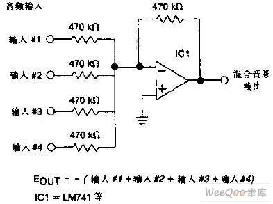
The picture shows a follower-type four-input audio mixer circuit. The circuit has four inputs. By adjusting the relative values of 470KM input resistor and 470KM feedback resistor, every input and every output will keep a gain of 1. (View)
View full Circuit Diagram | Comments | Reading(2200)
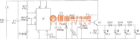
Microphone Low Noise Audio Preamplifier Circuit
Published:2011/7/18 6:50:00 Author:Sue | Keyword: Microphone, Low Noise, Audio, Preamplifier
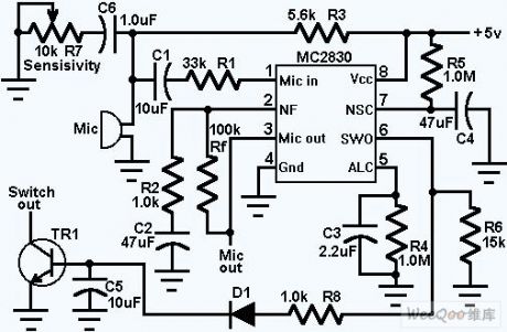
As seen in the figure, MC2830 will compose audio circuit. Traditional audio circuit cannot tell the difference between audio signal and noise signal. When it is very noisy, it is always the switch that make the noise. To avoid such disadvantage, we use different audio and noise wave forms. Audio wave form always has wide rangeability while noise wave form is more stable. Audio activation is decided by R6. If R6 changes from 14K to 0.7K, audio activation's sensibilitywill become lower. (View)
View full Circuit Diagram | Comments | Reading(1437)
DVD Player Power Circuit
Published:2011/7/14 7:20:00 Author:Sue | Keyword: DVD Player, Power
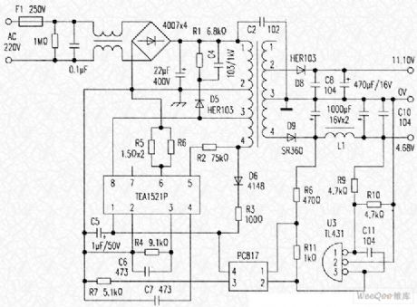
In DVD player power circuit, it is easy for TEA1521 toserve as flyback power.
(View)
View full Circuit Diagram | Comments | Reading(6698)
High-precision Analog Signal Isolating Amplifier
Published:2011/7/20 6:44:00 Author:Sue | Keyword: High-precision, Analog Signal, Isolating Amplifier, Isolating Operational Amplification, Isolating Operational Amplifier
Typical applications:
Direct current/voltage signal's isolation, transformation and amplication.
Industrial site signal's isolation and long-term transportation.
Analog signal's jamming and suppression of ground wire and statistics' isolation and collection.
Instruments and meters and sensor signal's reception and dispatch.
Non electrical quantity signal's conversion.
Power distribution, armarium's isolators.
Functions such as isolation of signal sensor's one-in-one-out, two-in-two-out of analog signal of 4-20mA.
ISO series optoelectronic isolation amplifier uses direct current signal imitation modulation technique. The null point and full scale within the range can be adjusted and set according to the sensor. (View)
View full Circuit Diagram | Comments | Reading(893)
Computer Mainboard ATXPWROK Control Circuit
Published:2011/7/19 7:52:00 Author:Sue | Keyword: Computer Mainboard, Control
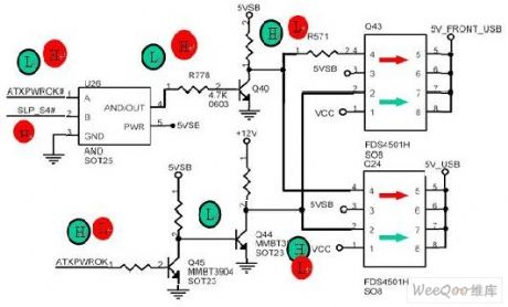
When it is working, ATXPWROK is high level. Q45 is connected and Q44 is disconnected. +12V voltage will be put on Q43 and Q24's pin 2 through resistors, that is binary channels MOS tube's N channel's control pin is high level and the channel is connected. At that time, VCC voltage will output 5V USB voltage from pin7,pin8 through N-type MOS tube. At the same time, when ATXPWROK is high level, ATXPWROK # is low level, then ANT GATE U26 outputs low level. Q40 is disconnected and will output high level control signal to Q43 and 24's pin 4, that is binary channel MOS tube's P-type channel is disconnected. Then pin 5, pin 6 have no output current, that is 5VSB doesn't supply 5VUSB voltage. (View)
View full Circuit Diagram | Comments | Reading(993)
The food humidity detector circuit (2)
Published:2011/7/21 0:21:00 Author:Borg | Keyword: humidity detector circuit
(View)
View full Circuit Diagram | Comments | Reading(826)
Balanced transmission mode circuit diagram
Published:2011/7/16 9:44:00 Author:Sophia | Keyword: Balanced transmission mode
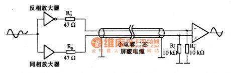
Figure is the balanced transmission mmode using twowire. This mode sends two signals with the 180 ° phase difference, and receive differeence of these two signals. Two signal lines can be offset if there is the noise between two signals. Balanced transmission is basically a low output impedance and high input impedance mode. The transmission line needs to use the two-wire shielded cable with excellent frequency characteristics and low distributed capacitance. (View)
View full Circuit Diagram | Comments | Reading(914)
CX2O111--the Am/Fm radio integrated circuit
Published:2011/7/15 19:14:00 Author:Borg | Keyword: Am/Fm radio, integrated circuit
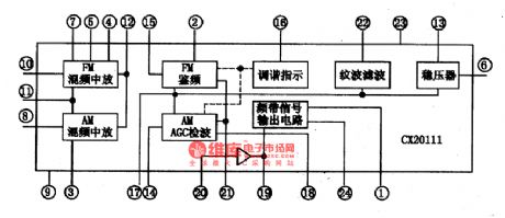

CX2O111 is the AM/FM radio integrated circuit produced by Sony, which is used in radios, recorders, compound stereos and so on.1.the internal circuit and pin functions of CX2O111CX2O111 includes all the circuits of the AM/FM and efficiency, mix, INTREQ and detected wave output audio signals. This IC is in 24-pin dual line flat package, whose internal circuit is shown in Figure 1 and the pin functions and data are listed in table 1.
Figure 1. the internal circuit of CX2O111
(View)
View full Circuit Diagram | Comments | Reading(2210)
TEANA A33-EL Electrical Load Signal Circuit One
Published:2011/7/14 8:43:00 Author:Joyce | Keyword: TEANA, Electrical Load , Signal
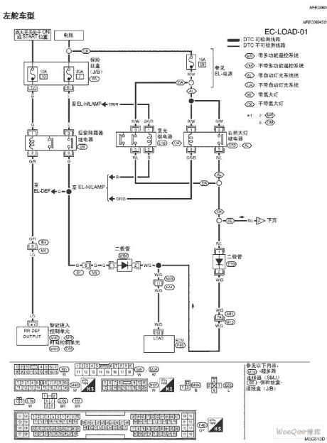
TEANA A33-EL Electrical Load Signal Circuit (View)
View full Circuit Diagram | Comments | Reading(807)
TEANA A33-EL Electrical Load Signal Circuit Two
Published:2011/7/14 8:43:00 Author:Joyce | Keyword: TEANA , Electrical Load , Signal
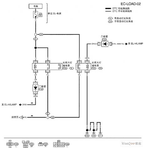
TEANA A33-EL Electrical Load Signal Circuit (View)
View full Circuit Diagram | Comments | Reading(851)
TEANA A33-EL Electrical Load Signal Circuit Three
Published:2011/7/14 8:43:00 Author:Joyce | Keyword: TEANA , Electrical Load , Signal
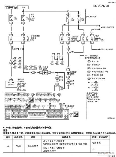
TEANA A33-EL Electrical Load Signal Circuit (View)
View full Circuit Diagram | Comments | Reading(776)
A 5W Frequency Modulation Transmitter Power Amplifier Circuit
Published:2011/7/20 3:16:00 Author:Joyce | Keyword: 5W , Frequency Modulation Transmitter, Power Amplifier

High frequency oscillation signal from output end IF of the varactor tuner of the television is used as the signal source. The tuner has a stable oscillation frequency, adding an 8 V voltage on input voltage BT would enable it to output stable frequency as long as the voltage is no less than 9 V. A coupling capacitance of several P should be added on the input end under operation. If the third stage amplifier gets too hot, two transistors should be connected with it in parallel .Adjusting the density of the inductance coil means adjusting the frequency-selecting loop.
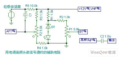 (View)
View full Circuit Diagram | Comments | Reading(1156)
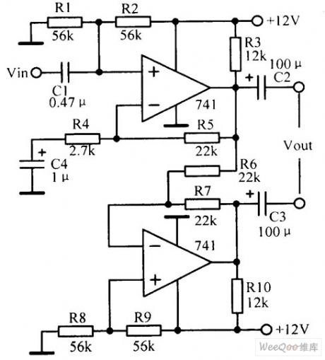
Mega Bass Circuit
Published:2011/7/20 3:16:00 Author:Joyce | Keyword: Mega Bass
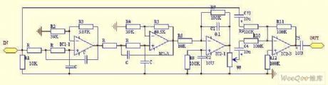
The mega bass circuit is as shown in the figure.
(View)
View full Circuit Diagram | Comments | Reading(3440)
| Pages:33/54 At 202122232425262728293031323334353637383940Under 20 |
Circuit Categories
power supply circuit
Amplifier Circuit
Basic Circuit
LED and Light Circuit
Sensor Circuit
Signal Processing
Electrical Equipment Circuit
Control Circuit
Remote Control Circuit
A/D-D/A Converter Circuit
Audio Circuit
Measuring and Test Circuit
Communication Circuit
Computer-Related Circuit
555 Circuit
Automotive Circuit
Repairing Circuit