
Control Circuit
Index 151
ELECTROMETER_AMPLIFIER_WITH_OVERLOAD_PROTECTION
Published:2009/7/1 4:22:00 Author:May
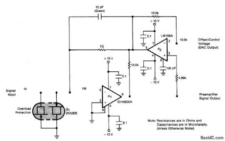
The preamplifier is protected from excessive input signals of either polarity by the 2N5909 junction field-effect transistor. A nulling circuit makes it possible to set the preamplifier output voltage to zero at a ftxed low level (up to ±10-8A) of the input current. (This level is called the standing current and corresponds to the zero-signal level of the instrumentation.) The opposing (offset) current is generated in the 109 feedback resistor to buck the standing current. Different current ranges are reached by feeding the preamplifter output to low and high gain amplifter chains. To reduce noise, each chain includes a 1.5 Hz corner active filter. (View)
View full Circuit Diagram | Comments | Reading(1433)
HIGH_CURRENT_HIGH_SPEED_SWITCH
Published:2009/7/24 3:54:00 Author:Jessie

Alloy junction transistor (2N2648 germanium) has useful frequency range up to 10 Mc for switching up to 1 amp with gain of 50 in 0.8 microsec.-Medium Power Transistor Has Multiple Uses, Electronics, 361, p 132. (View)
View full Circuit Diagram | Comments | Reading(1024)
SPEAKER_OVERLOAD_PROTECTOR
Published:2009/7/1 4:22:00 Author:May
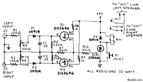
The input to the circuit is taken from the amplifier's speaker-output terminals or jacks. If the right-channel signal is sufficiently large to charge C1 to a potential that is greater than the breakdown voltage of Q1's emitter, a voltage pulse will appear across R7. Similarly, if the left-channel signal is sufftciently large to charge C2 to a potential that is greater than the breakdown voltage of Q2's emitter, a pulse will appear across R7. The pulse across R7 triggers SCR1, a sensitive gate SCR (IGT less than 15 mA where IGT is the gate trigger-current), that latches in a conducting state and energizes RY1. The action of the relay will interrupt both speaker circuits, and the resulting silence should alert you to the problem. Cut back the volume on your amplifier, then press and release S1 to reset the circuit and restore normal operation. The circuit can be adjusted to trip at any level from 15 to 150 watts RMS. To calibrate, deliberately feed an excessive signal to the right input of the speaker protector and adjust R3 until RY1 energizes. Do the same with the left channel, this time adjusting R4. The circuit is now calibrated and ready for use. (View)
View full Circuit Diagram | Comments | Reading(1324)
SCS_CONTACT_ISOLATOR
Published:2009/7/24 3:53:00 Author:Jessie
Eliminates contact bounce in grounded-switch arrangement where switch is opened to trigger scs.- transistor Manual, Seventh Edition, General Electric Co., 1964, p 433. (View)
View full Circuit Diagram | Comments | Reading(613)
10_KV_SWITCHING_CIRCUIT
Published:2009/7/24 3:53:00 Author:Jessie
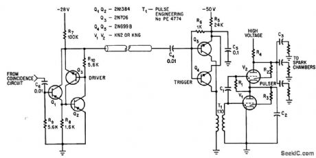
Cold-cathode gas tubes provide reliable switching of high voltage to army of spark chambers in bal-loon-borne equipment. Three-transistor line driver can be to feet away. Negative pulse input to Q1 makes Q2 and Q3 go into regenerative mode, discharging C4 to turn on trigger that applies 500 V to ire pulser.-R. E. Daniels and A. D. Cook, Cold-Cathode Gas Tubes Switch High Voltage Fast, Electronics, 37:14, p 72-73. (View)
View full Circuit Diagram | Comments | Reading(759)
THREE_DIODE_SWITCH_FOR_VIDEO_TIME_SHARING
Published:2009/7/24 3:52:00 Author:Jessie
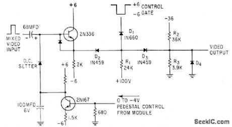
Gate pulse applied to diode D1draws current from R1 through D1 (switch open) or through D2 and D3 (switch closed so video passes from input to output). Clamp diode D4 keeps base line of output always positive.-T. Vagt, New Light on Air Traffic: Bright Plan Display with Alphanumerics, Electronics, 36:30, p 42-46. (View)
View full Circuit Diagram | Comments | Reading(701)
SWITCHING_CAPACITANCE_TRANSDUCERS
Published:2009/7/24 4:00:00 Author:Jessie
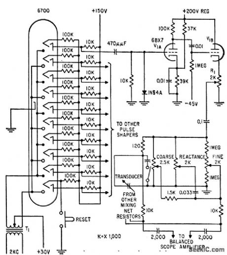
Beam-switching tube pulses bridges sequentially. Each bridge has pressure-sensitive capacitance transducer that unbalances bridge in proportion to changes in pressure. Outputs of bridges are displayed as pulse pattern corresponding to pattern of pressure imposed on auto seat.-A. Stiebel, High-Speed Switching of Low level Signals, Electronics, 32:12, p 54-55.
(View)
View full Circuit Diagram | Comments | Reading(633)
HIGH_SPEED_TRANSISTOR_RELAY
Published:2009/7/24 3:58:00 Author:Jessie
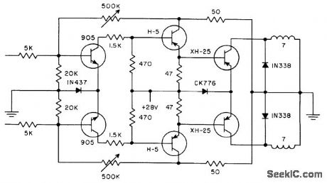
Push-pull switch handles up to 10 amp with rise time of 50 microsec. Rising d-c voltage at input produces no output until predetermined level is reached, when power supply voltage is suddenly switched across load. Circuit remains locked in until input voltage drops below trip level. Trip voltage is determined largely by breakdown voltage of 1N437 zener diode.-D. L. Anderson, Fast Transistor Relay, Electronics, 31:11, p 145. (View)
View full Circuit Diagram | Comments | Reading(798)
FAST_INDUCTIVE_SWITCHING
Published:2009/7/24 3:58:00 Author:Jessie
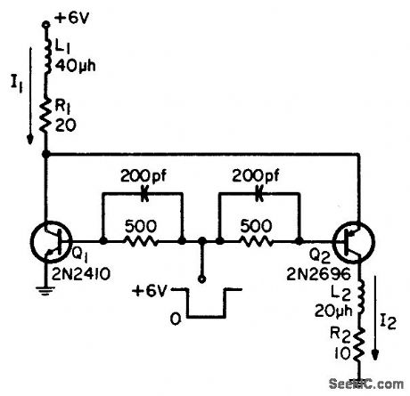
Fast-rise current switching circuit provides current as fast as it can be switched into highly inductive load. Used as current driver for digital com purer memory arrays as well as for speeding up ordinary relays.-T. W. Collins, Fast-Rise Current Switch, FEE, 13:1, p 65-66. (View)
View full Circuit Diagram | Comments | Reading(694)
ELECTRONIC_R_F_SWITCH
Published:2009/7/24 3:57:00 Author:Jessie
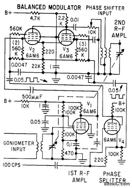
V1 isolates gonio-meter from balanced modulator lubes V2 and V3, which provide 90° phase shift of gonio-meter signal. V2 and V3 are made to conduct alternately by 100-cpsdrive applied to their suppressor grids by phase-splitter V4.-J. F. Hatch and D. W. G. Byatt, Direction Finder with Automatic Readout, Electronics, 32:16, p 52-54. (View)
View full Circuit Diagram | Comments | Reading(707)
SPARK_GAP_SWITCH
Published:2009/7/24 3:56:00 Author:Jessie
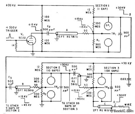
Bank of 111 spark gaps switches 30 kV in less thon 10 millimicrosec, to explode wire for generating plasma in shock tube or generating hypersonic waves in wind tunnel. Jitter problem is solved by using one spark gap to trigger another. Thyratron V1 fires section 1 having single gap, and this triggers 10 gaps in section 2, each of which in turn triggers 10 gaps in section 3.-H. B. McFarlane, Spark Gaps for Fast High-Voltage Switching, Electronics, 32:31, p 72-73. (View)
View full Circuit Diagram | Comments | Reading(1433)
ALARM_CIRCUIT
Published:2009/7/1 3:43:00 Author:May
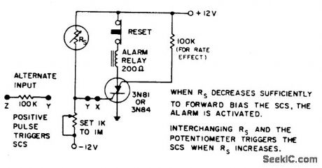
Temperature, light, or radiation sensitive resistors up to 1 megohm readily trigger the alarm when they drop below the value of the preset potentiometer. Alternately, 0.75 V at the input to the 100 kΩ triggers the alarm. Connecting SCS between ground and -12 V permits triggering on negative input to GA. (View)
View full Circuit Diagram | Comments | Reading(955)
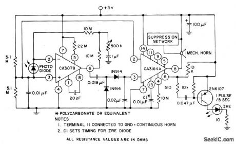
PHOTOELECTRIC_ALARM_SYSTEM
Published:2009/7/1 3:42:00 Author:May

The CA3164A BiMOS detector alarm system and the CA3078 micropower op amp with a photodiode are used as an automatic switch for turning on a night light or sounding a mechanical horn. (View)
View full Circuit Diagram | Comments | Reading(1141)
CROWBAR
Published:2009/7/24 4:06:00 Author:Jessie
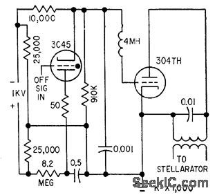
Used to cut off oscillator sharply in lank circuit of stellarator. Consists of lube with plate holdoff rating comparable to peak instantaneous output tank voltage. At end of pulse, grid is driven to +500 V end tube becomes low impedance across lank, to damp out oscillation within a cycle or two.-R. t. Gamblin, Radio-Frequency Circuits for Plasma Physics, Electronics, 32:27, p 50-52. (View)
View full Circuit Diagram | Comments | Reading(1)
ROW_STORAGE_UNIT_FOR_MAGNETIC_CONTOUR_DISPLAY
Published:2009/7/24 4:06:00 Author:Jessie
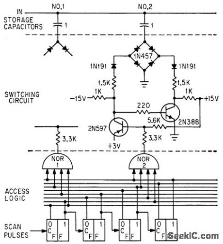
Scan pulses activate nor gates in sequence. For 11 by 11 display matrix, there are 11 nor pates each with its switching circuit. On read-in, nor gate output of -10 V activates switching circuit, grounding its capacitor and making capacitor charge up to value of that data point.-W. W. Anderson, Latest Antisubmarine Aid-Magnetic Contour Display System, Electronics, 36:32, p 58-61. (View)
View full Circuit Diagram | Comments | Reading(722)
ELECTRIC_FISH_FENCE
Published:2009/7/24 4:05:00 Author:Jessie
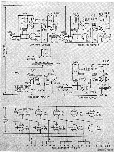
Output of 360-kw d-c generator is applied to row of electrodes in sequence by pair of high. voltage ignitron tubes that runt pulse on and off for each electrode in turn. Single turnoff ignitron terminates pulse period of whichever loaded ignitrons are conducting.-C. D Volz, Ignitron-Pulsed Electric Fence Guides Migrating Salmon, Electronics, 35:16, p 50-52. (View)
View full Circuit Diagram | Comments | Reading(1258)
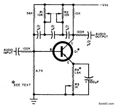
DIFFERENTIAL_VOLTAGE_OR_CURRENT_ALARM
Published:2009/7/1 3:39:00 Author:May
The input may be dc or low frequency ac,The output is a distinctive senes of audiobeeps or a continuous tone,and occurs only when a selected polarity unbalance IS pres-ent at the mput. (View)
View full Circuit Diagram | Comments | Reading(774)
MULTIPLE_ALARM_CIRCUIT
Published:2009/7/1 3:38:00 Author:May
Any of several inputs pulls in the common alarm relay with lamps giving visual indication of triggering input. Low resistance lamps decrease input sensitivity. (View)
View full Circuit Diagram | Comments | Reading(977)
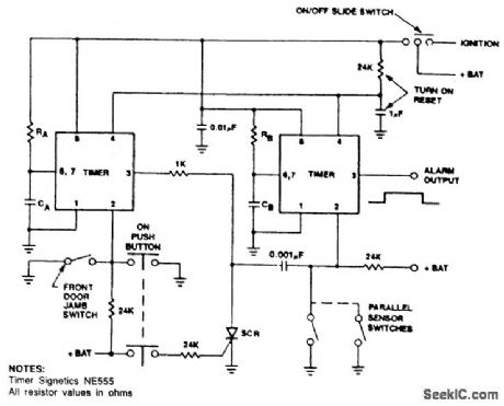
AUTO_BURGLAR_ALARM
Published:2009/7/1 3:37:00 Author:May
Timer A produces a safeguard delay, allowing the driver to disarm the alarm and eliminating a vulnerable outside control switch. The SCR prevents timer A from triggering timer B, unless timer B is triggered by strategically-located sensor switches. (View)
View full Circuit Diagram | Comments | Reading(0)
SIMPLE_24_h_CLOCK
Published:2009/7/1 3:29:00 Author:May
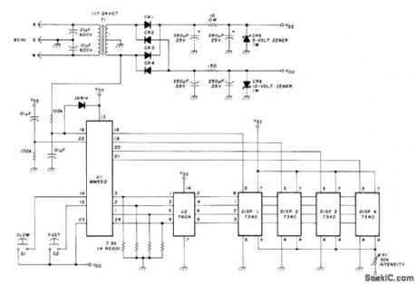
Use of 60-Hz power frequency as time base simplifies design while still giving Iong-term accuracy comparable to that of crystal time base. Four-digit display uses Hewlett-Packard 5082-7340 displays requiring only simple four-Iine BCD input. National MM5312N IC divides Iine frequency down to one pulse per minute and advances its internal storage register at same rate. Output of register is in binary form at pins 1, 2, 3, and 24, synchronized with digit-enable outputs at pins 18, 19, 20, and 21. Binary data is thus applied to all four displays in parallel, with enable lines controlling data feed. SN7404N inverter converts binary output data to TTL level required by displays.Power supply provides +5 V and -12 V for ICs and 60-Hz reference for clock check. CR5 is Radio Shack 276-561, CR6 is 276-563, and CR1-4 are 276-1146.-K. Powell, 24-Hour Clock with Digital Readout and Line-Frequency Time Base, Ham Radio, March 1977, p 44-48
(View)
View full Circuit Diagram | Comments | Reading(1696)
| Pages:151/312 At 20141142143144145146147148149150151152153154155156157158159160Under 20 |
Circuit Categories
power supply circuit
Amplifier Circuit
Basic Circuit
LED and Light Circuit
Sensor Circuit
Signal Processing
Electrical Equipment Circuit
Control Circuit
Remote Control Circuit
A/D-D/A Converter Circuit
Audio Circuit
Measuring and Test Circuit
Communication Circuit
Computer-Related Circuit
555 Circuit
Automotive Circuit
Repairing Circuit