
Control Circuit
Index 147
DIGITAL_CONTROL_T0_100_kHz
Published:2009/7/2 7:30:00 Author:May
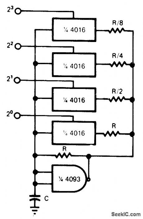
Schmitt trig-ger function of CD4093B IC gives oscillator op-eration over four decades of frequency without changing C. Basic frequency value is equal to kl RC, with k equal to 1.3 up to about 5 kHz and decreasing gradually to 1.0 at 100 kHz. Use of CD4016 quad transmission gate permits remote switching in of additional resistors to provide direct digital control of frequency. Arrangement shown gives choice of five unrelated frequen-cies, but binary selection of binary-weighted re-sistors witl give choice of 16 unrelated frequen-cies.-R. Tenny, CMOS Oscillator Features Digital Frequency Control, EDNMagazine, June 5, 1976, p 114 and 116. (View)
View full Circuit Diagram | Comments | Reading(770)
Simple_differential_thermometer
Published:2009/7/24 2:16:00 Author:Jessie
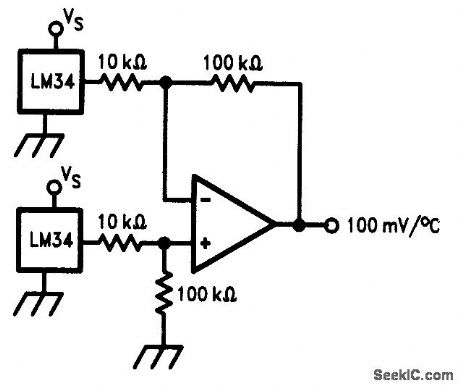
Fig. 13-12 This circuit produces an output voltage that is proportional to the temperature difference between the two LM34s. The difference amplifier sub-tracts the LM34 outputs from one another and then multiplies the difference by a factor of 10 to provide a single-ended output of 100 mV/°F of differential temperature. National Semiconductor Linear Applications Handbook 1991, p 1079. (View)
View full Circuit Diagram | Comments | Reading(778)
Proportional_temperature_controller
Published:2009/7/24 2:16:00 Author:Jessie
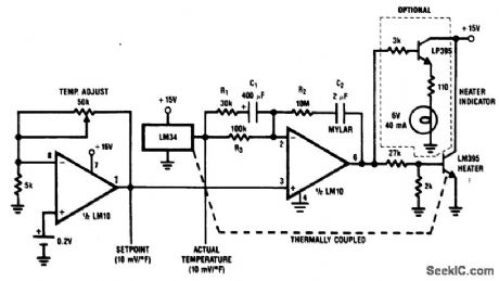
Fig. 13-11 Here, an LM10 serves as both a temperature-setting device and as a driver for the heating unit (an LM395 power transistor). The optional lamp, driven by an LP395, indicates if power is applied to the heater. When a change in temperature is desired, the user adjusts the 50-kΩ pot and the circuit makes the temperature transition with a minimum of overshoot or ringing. The circuit is calibrated by selection of R2, R3, and C2 for minimum overshoot. C2 eliminates dc offset errors. R1 and C1 are added to improve loop stability about the temperature-set point. For optimum performance, locate the temperature sensor LM34 as close as possible to the heater. This will minimize time lag between the heater and sensing. Long-term stability and repeatability are better than 0.5°F. National Semiconductor Linear Applications Handbook, 1991. p 1079 (View)
View full Circuit Diagram | Comments | Reading(0)
PWN_MOTOR_SPEED_CONTROL
Published:2009/7/2 5:15:00 Author:May
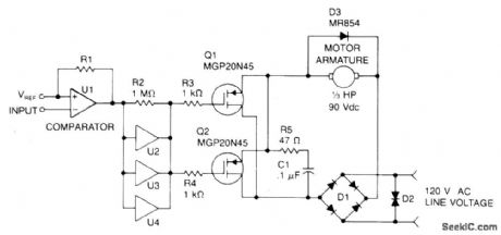
Speed control is accomplished by pulse width modulating the gates of two MGP20N45 TMOS devices. Therefore, motor speed is proportional to the pulse width of the incoming digital signal, which can be generated by a microprocessor or digital logic.The incoming signal is applied to comparator U1, then to paralleled inverters U2, U3, and U4 that drive the two TMOS devices, which, in turn, control power applied to the motor armature. Bridge rectifier Dl supplies fullwave power that is filtered by R5 and C1. Free-wheeling diode D3 (MR854) prevents high voltage across Q1 and Q2.A back-to-back zener diode, D2, protects against transients and high voltage surges. (View)
View full Circuit Diagram | Comments | Reading(882)
AF_NOISE_LlMlTER_1
Published:2009/7/2 4:54:00 Author:May
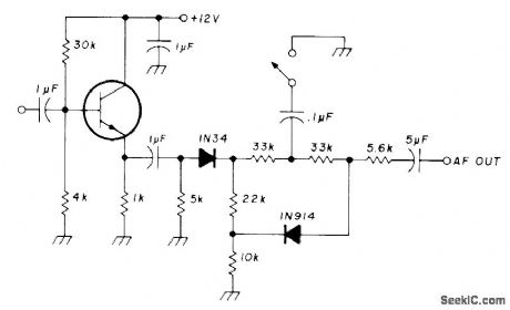
Operation is similar to that of delay line. Voltage developed across voltage divider at output of 1N34 germanium diode is instantaneous, while DC voltage at output of circuit is delayed. If no pulses are present and 0.1-μF capacitor is not at ground, 1N914 silicon diode will have floating voltage. High positive pulses charge capacitor, and silicon diode shorts audio voltage. Negative pulses disable germanium diode directly. Circuit thus acts as noise blanker in both directions. Used in European communication receivers. Transistor type is not criticaL-U. L. Rohde, IF Amplifier Design. Ham Radio, March 1977. p 10-21. (View)
View full Circuit Diagram | Comments | Reading(621)
Cold_junction_compensation_for_the_type_K_thermocouple
Published:2009/7/24 2:21:00 Author:Jessie
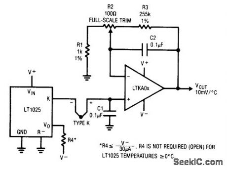
Fig. 13-15 This circuit is similar to that of Fig. 13-14, except that a type-K thermocouple subtracts from the LT1025 in series-opposed fashion. The net result is fed to the amplifier. Optional pull-down resistor R4 allows readings below 0℃. Linear Technology, Linear Applications Handbook 1990 p AN28-5. (View)
View full Circuit Diagram | Comments | Reading(706)
THIN_FOIL_WELD_CONTROL
Published:2009/7/24 2:20:00 Author:Jessie
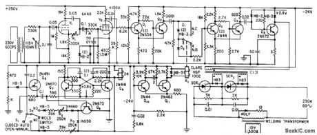
Control circuit uses gated rectifiers to generate welding pulses for rates up to 15 welds per second in foils up to 10 mils thick.-D. D. Kline, Automatic Welder for Thin Foils,Electronics,33:36,p 48:49. (View)
View full Circuit Diagram | Comments | Reading(770)
AUTO_FADE
Published:2009/7/2 4:30:00 Author:May
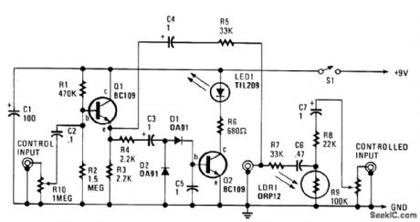
The automatic fader drops the level of the background music when the narration comes up. The control input goes through R10, a preset audio level control, to the input of an emitter-follower buffer stage (Q1). The buffer offers a high input impedance and makes sure that the source impedance is low enough to drive the rectifier and smoothing circuit, which consist of D1, D2, and C5. The smoothed output drives a simple LED circuit. R8 and LDR1 form an input attenuator across which the output is fed via C6 and C7 to the output jack. The output at the emitter of Q1 couples to this socket through C4 and R5. R5 and R7 are a passive mixer. With 200 mV or less at the input, there isn't sufficient voltage across C5 to make Q2 turn on. Over 200 mV, Q2 does turn on to a limit, and the LED gets power. That makes the LDR's resistance fall, and signal loss through the attenuator increases. Increase the input to 350 mV rms, and you get a signal reduction of better than 20 dB. (View)
View full Circuit Diagram | Comments | Reading(1203)
TIME_DELAY_SWITCH
Published:2009/7/2 4:30:00 Author:May
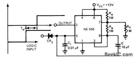
Oscillator connection shown for 555 timer provides delay for switching action controlled by logic input. When logic input is 0 V, timer output is low. When logic input goes high, output remains low for delayof 0.693RBC s and then switches high. Output remains high as long as input is high.-K. D.Dighe, Rearranged Components Cut 555's lnitial-Pulse Errors, EDNMagazine, Jan. 5, 1978, p 82 and 84. (View)
View full Circuit Diagram | Comments | Reading(1033)
POWER_UP_POWER_DOWN_RESET
Published:2009/7/2 4:26:00 Author:May
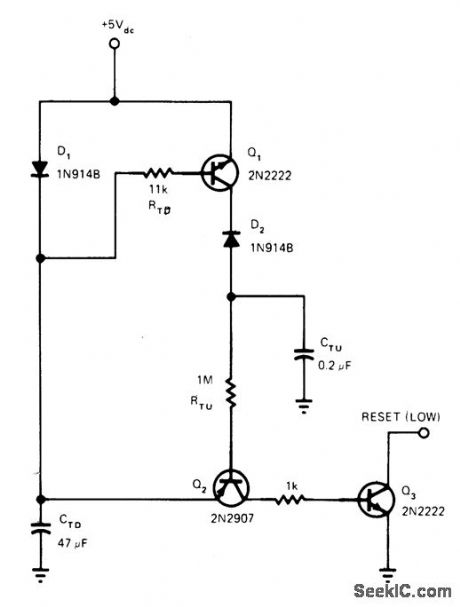
Output of circuit goes high at end of time interval RTUCTU, required for charging of CTU by applied 5-VDC inputsignal. When 5-V power fails, Q1, drives Q2, and Q3, off, making output low for time interval determined by RTDCTD. When CTD is discharged, output goes high again. Interruption of power thus produces negative-going pulse having variable width determined by values chosen for resistors and capacitors.-S. Rummel, Reset Circuit Detects Power Drop-Out, EDN Magazine, May 20, 1976, p 94. (View)
View full Circuit Diagram | Comments | Reading(1037)
NOISE_CONTROL
Published:2009/7/2 4:21:00 Author:May
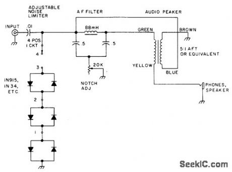
Circuit is plugged into headphone jack of amateur receiver. Four-position rotary switch selects desired combination of noise-limitingdiodes for handling progressively more severe noise pulses. Adjustable AF T-notch filter limits passband over sufficient range for both phone and CW. Inductor is common 88-mH toroid. Audio peaker circuit overcomes insertion losses of filters.-S. T. Rappold. Noise Rejector. 73 Magazine. Sept. 1977. p 116. (View)
View full Circuit Diagram | Comments | Reading(787)
CURRENT_SLOPE_CONTROL_FOR_RESISTANCE_WELDING
Published:2009/7/24 2:25:00 Author:Jessie
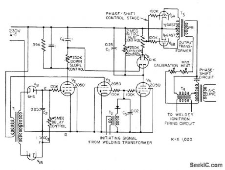
Varies buildup and decay rates of, current, to increase weld quality and uniformity. Consists essentially of variable resistance inserted in phase-shift circuit of main welding control.-J. Markus and V. Zeluff, Handbook of Industrial Electronic Control Circuits, McGraw-Hill, New York, 1956, p 340. (View)
View full Circuit Diagram | Comments | Reading(1316)
Differential_sensing_for_type_J_grounded_thermocouple
Published:2009/7/24 2:25:00 Author:Jessie
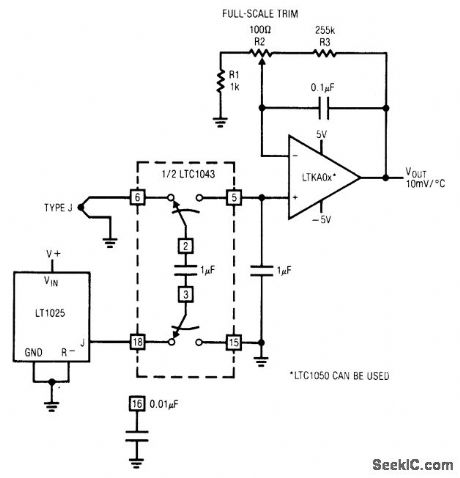
Fig. 13-17 This circuit also provides full-differential sensing as in Fig, 13-16, but for type-J grounded thermocouples.Note that the sensor output is subtracted from the LT1025. Linear Technology Linea Applications Handbook 1990 p AN28-7. (View)
View full Circuit Diagram | Comments | Reading(900)
AC_MOTOR_CONTROL
Published:2009/7/2 4:19:00 Author:May
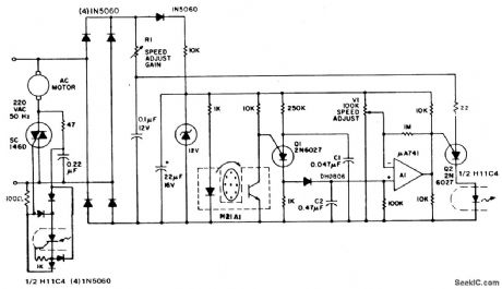
The circuit illustrates feedback speed regulation of a standard ac induction motor, a function difficult to accomplish other than with a costly, generator type, precision tachometer. When the apertured disc attached to the motor shaft allows the light beam to cross the interrupter module, the programmable unijunction transistor, Q1, discharges capacitor, C1, into the much larger storage capacitor, C2. The voltage on C2 is a direct function of the rotational speed of the motor. Subsequently, this speed-related potential is compared against an adjustable reference voltage, V1, through the monolithic operational amplifier, A1, whose output, in turn, establishes a dc control input to the second P.U.T.(Q2). This latter device is synchronized to the ac supply frequency and furnishes trigger pulses in the conventional manner to the triac at a phase angle determined by the speed control, R1, and by the actual speed of the motor. (View)
View full Circuit Diagram | Comments | Reading(3144)
Differential_sensing_for_the_type_K_thermocouple
Published:2009/7/24 2:23:00 Author:Jessie
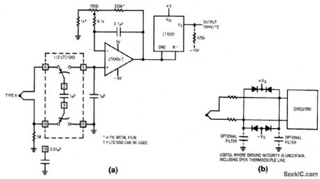
Fig. 13-16 This circuit combines full-differential sensing and filtering for a type-K thermocouple. The circuit has 120-dB dc common-mode rejection if all signals remain within the LTC1043 supply-voltage range. The LTC switched-capacitor building block transfers charge between the input flying capacitor and the output capacitor. The LTC1043 commutating frequency, which is settable, controls the rate of charge (and hence the overall bandwidth). The differential inputs reject noise and common-mode voltages (within the LTC1043 supply range). Excursions outside these limits require protection networks, as shown in Fig. 13-16B. As in Fig. 13-15, the optional pull-down resistor permits negative readings. The 1-MΩ resistor provides a bias path for the LTC1043 floating inputs. Linear Technology. Linear Applications Handbook 1990 p AN28-6. (View)
View full Circuit Diagram | Comments | Reading(917)
Centigrade_thermometer_with_cold_junction_compensation
Published:2009/7/24 3:08:00 Author:Jessie
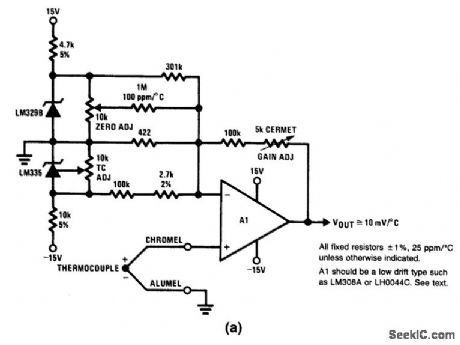
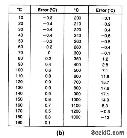
Fig. 13-40 This circuit is an electronic thermometer with a 10 mV/℃ output from 0℃ to 1300℃. To trim, first short out the LM329B, the LM335 and the thermocouple. Measure and record the output voltage from A1 (this should be equal to the input offset voltage of A1 times the voltage gain). Remove the short from the thermocouple and apply a 50-mV input to A1 and adjust the 5-kΩ gain potentiometer until the A1 output voltage is 12.25 V above the previously recorded value. Short out the thermocouple again, but remove the short across the LM335. Adjust the 10-kΩ TC potentiometer so that the output voltage from A1 equals 10 mV/°K times the absolute temperature. Finally, remove the short across the LM329B and adjust the 10-kΩ zero potentiometer so that the A1 output voltage equals 10 mV/℃ times the ambient temperature in 0℃. The table of Fig. 13-40B shows the error resulting from thermocouple nonlinearity as a function of temperature. National Semiconductor Linear Applications Handbook 1991, p. 524, 525. (View)
View full Circuit Diagram | Comments | Reading(3422)
Temperature_controller_for_quartz_crystal_ovens
Published:2009/7/24 2:59:00 Author:Jessie
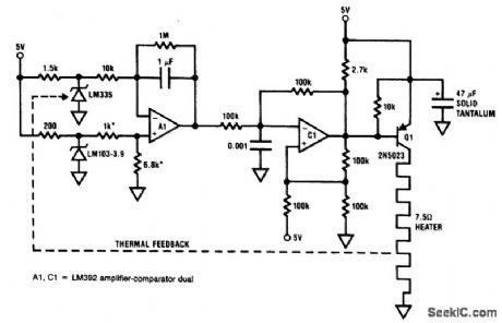
Fig. 13-35 This circuit will provide temperature control for an oven at 75℃, which is ideal for most types of quartz crystals. The temperature setpoint is established by the LM103-3.9 reference and the 1- to 6.8-kΩ divider. In practice, the LM335 should be in good thermal contact with the heater to prevent servo oscillation. National Semiconductor. Linear Applications Handbook 1991 p 839. (View)
View full Circuit Diagram | Comments | Reading(1672)
Thermistor_signal_conditioner_for_current_loops
Published:2009/7/24 2:48:00 Author:Jessie
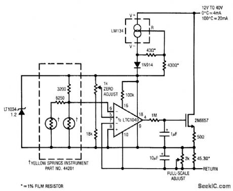
Fig. 13-28 This circuit shows a complete 2-wire thermistor temperature-transducer interface with a 4- to 20-mA output. The 4- to 20-mA current-loop control is common in industrial environments. The circuits used to modulate transducer data in a 4- to 20-mA loop must operate well below the 4-mA minimum current. Over a 0 to 100℃ range, accuracy is ±0.3℃ and the circuit is current-loop powered (no external supply is required). Trims shown are for 0℃ and 100℃, and are made by exposing the thermistors to those temperatures. The thermistor datasheets show methods for electrically simulating 0℃ and 100℃, Linear Technology Linear Applications Handbook, 1990 p AN23-5 . (View)
View full Circuit Diagram | Comments | Reading(1446)
DOPPLER_BURGLAR_ALARM
Published:2009/7/2 3:34:00 Author:May
Small radar transmitter operating at 10.687 GHz fills pro-tected area with radio waves. Waves reflected from stationary objects are ignored by receiver, while waves undergoing Doppler shift in fre-quency by reflection from moving object such as intruder are selectively amplified for trigger-ing of alarm. Single waveguide section is di-vided into two cavities, each having Gunn diode; transmitter cavity feeds points A and B of transmitter TR7-IC3, and other cavity feeds points C and D of amplifier that drives alarm relay. Article covers construction and operation of circuit and gives sources (British) for parts and construction khs. Opamps are SN72748 or equivalent, IC3 is μA723 or equivalent, Tr1-Tr3 are ZTX500 or equivalent, Tr4-Tr6 are ZTX302 or equivalent, Tr7 is 3055, D1-D8 are 1N4001 or equivalent, D9-D10 are 1N914, SCR1 is TIC44 or equivalent, Z1-Z2 are BZY88-C8V2, relay is 18-V with 1K coil, Doppler module is Mullard CL8960 or equivalent, and seff-oscillating mixer for re-ceiver is Mullard CL8630S or equivalent. Alarm stays on until reset by appropriate swhch.-M.W. Hosking, Microwave Intruder Alarm, Wire-less World, July 1977, p 36-39. (View)
View full Circuit Diagram | Comments | Reading(1616)
SOUND_ACTIVATED_SWITCH
Published:2009/7/2 3:20:00 Author:May
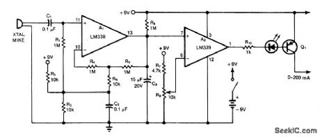
Can be used as sensor for burglar alarm or for turning on su'-veillance tape recorder to monitor conversa-tions. R8, is adjusted to give desired sensitivity at which A2, triggers switch Q1, to provide 200-mA load current and turn on indicator LED. First section of LM339 quad comparator serves as amplifier and detector providing gain of 100. Second comparator compares DC output of first with reference level selected by R8.-D. ft. Mor-gan, Sound Turns Switch On, EDN Magazine, Aug. 5, 1978, p 82 and 84. (View)
View full Circuit Diagram | Comments | Reading(3368)
| Pages:147/312 At 20141142143144145146147148149150151152153154155156157158159160Under 20 |
Circuit Categories
power supply circuit
Amplifier Circuit
Basic Circuit
LED and Light Circuit
Sensor Circuit
Signal Processing
Electrical Equipment Circuit
Control Circuit
Remote Control Circuit
A/D-D/A Converter Circuit
Audio Circuit
Measuring and Test Circuit
Communication Circuit
Computer-Related Circuit
555 Circuit
Automotive Circuit
Repairing Circuit