
Control Circuit
Index 146
Micropower_thermometer
Published:2009/7/24 3:10:00 Author:Jessie
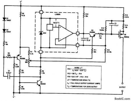
Fig. 13-41 The output of this circuit is a current proportional to temperature, which can be used to drive a meter for a direct readout. Alternatively, a resistor or op amp can be used to get a voltage output. The circuit is pulsed at a low duty cycle to reduce power consumption. With the component shown, the duty cycle is about 0.2% with a one-second sample rate. This gives an average current drain of about 25μA, plus the output current. The circuit will operate with a supply of 8.0 to 12.0 V. A small 8. 4-V mercury battery can provide an operating life of about one year. R8 is used to trim the circuit, correct for Zener tolerance, temperature error in the sensor, and resistor tolerance. With the values shown, a 0- to 50-μA output is obtained for a +50 to + 100°F temperature change. Other ranges can be selected using the equations shown in the box on the circuit diagram. The current-source output allows long lines to be driven with no loss of accuracy. National Semiconductor Linear Applications Habdbook, 1991, p. 1229.
(View)
View full Circuit Diagram | Comments | Reading(1)
Relative_humidity_sensor
Published:2009/7/24 2:34:00 Author:Jessie

Fig, 13-20 This circuit combines two LTC1043 switched-capacitor building blocks with a capacitive-based humidity transducer (Parametrics #RHS) to provide full signal conditioning for a relative-humidity output. To calibrate, place the sensor in a known 5% relative-humidity environment, and adjust the 10-kΩ 5% RHtrim for a 0.05-V output. Next, place the sensor in a 90% relative-humidity environment and set the 500-Ω 90% RH trim for 900-mV output. Repeat this procedure until both points are fixed. Once calibrated, this circuit is accurate within 2%on the 5 to 90%alative-humidity range.Linear Technology Linear Applications Handbook, 1990.
(View)
View full Circuit Diagram | Comments | Reading(1026)
OPEN_SHORT_GROUND_ALARM
Published:2009/7/2 23:25:00 Author:May
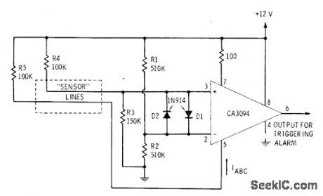
Pin 6 of CA3094 IC is high for no-alarm condition. When any one sensor line is open, is shorted to other line, or is shorted to ground, output of IC goes low and resulting output current serves for activating alarm system.-E. M. Noll, Linear IC Principles, Experiments, and Projects, Howard W. Sams, Indianapolis, IN, 1974, p 316-317. (View)
View full Circuit Diagram | Comments | Reading(863)
TEMPERATURE_COMPENSATED_OFFSET_CONTROL
Published:2009/7/2 21:54:00 Author:May
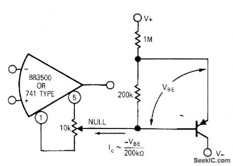
Drift effects of offset adjustment are removed by deriving correction current from emitter-base voltage of PNP signal transistor to develop appropriate temperature compensatioll. Correction current is divided with conventional control pot used for adjusting offset voltage. Article gives design equations.-J.Graeme, Offset Null Techniques Increase Op Amp Drift, EDN Magazine. Aprill. 1971. p 47-48. (View)
View full Circuit Diagram | Comments | Reading(869)
Cold_junction_compensation_for_the_type_J_thermocouple
Published:2009/7/24 2:19:00 Author:Jessie
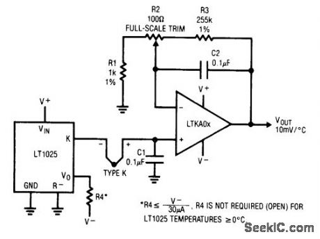
Fig. 13-14 This circuit uses an LT1025 and an LT1001 to provide a scaled, cold-junction-compensated output. R6 is a typical value and it might require selection to accommodate the R5 trim range. Alternately, R6 can be re-scaled, and R5 enlarged (with some penalty in trim resolution). Linear Technology Linear Applications Handbook 1990 p. AN28-4. (View)
View full Circuit Diagram | Comments | Reading(939)
LATCHING_ALARM
Published:2009/7/2 20:43:00 Author:May
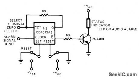
Single-channel monitorusing half of CD4013AE flip-flop detects out-of-tolerance condition or alarm state representedby logic 1 on dockinput Flip-flop then changesto alarm state that turns on transistor for energizing alarm device,and holds alarm condition until operator reacts by applying voltage to SET input,Logic 0 on D terminal activates flip-flop when monitoring is desired.-J,C Nichols,CMOS D Flop Makes Latching AND Gate.EDN Magazine,April 20, 1974,p 89 and 91. (View)
View full Circuit Diagram | Comments | Reading(0)
Extended_range_Fahrenheit_temperature_sensor_dual_supply
Published:2009/7/24 1:58:00 Author:Jessie

Fig. 13-3 This circuit is similar to that of Fig. 13-1, except that the temperature range is extended, -50° to +300°F, using a dual supply. Note that R1 must be selected to provide 50μA with the available -Vsupply. National Semiconductor. Linear Applications Handbk.1991 p. 1076 (View)
View full Circuit Diagram | Comments | Reading(580)
Extended_range_Fahrenheit_temperature_sensor_single_supply
Published:2009/7/24 1:57:00 Author:Jessie
Fig, 13-2 This circuit is similar to that of Fig. 13-1, except that the temperature range is extended, -50° to +300°F, using a single supply. National Semiconductor, Linear Applications Handbook 1991. p 1076. (View)
View full Circuit Diagram | Comments | Reading(564)
Basic_Fahrenheit_temperature_sensor
Published:2009/7/24 1:55:00 Author:Jessie
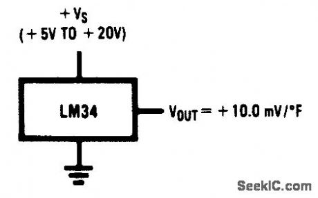
Fig. 13-1 This simple circuit requires only one three-terminal LM34, and produces an output voltage directly related to temperature. For example, if Vout is 0.72 V, the temperature is 72°F. Accuracy is ±0.4°F. The TO-46 package can be cemented or soldered to the mounting surface. If soldered to a metal surface, the ground pin is at the surface potential. If heat fins are used, thermal response time is speeded up. If soldered to a thermal mass, the reading will be steady despite small changes in temperature. National Semiconductor Linear Applications Handbook 1991, p 1076, (View)
View full Circuit Diagram | Comments | Reading(0)
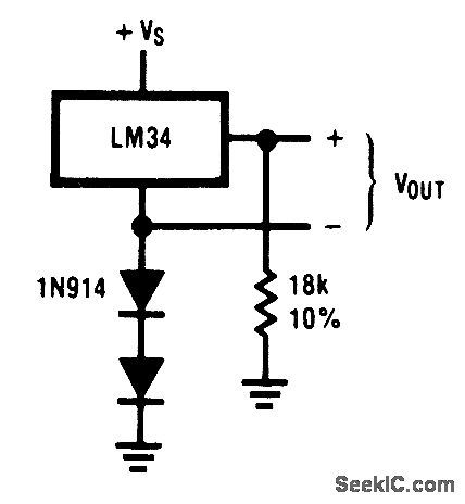
Remote_temperature_sensor_grounded_sensor
Published:2009/7/24 2:04:00 Author:Jessie
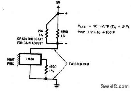
Fig. 13-4 This circuit uses the basic LM34 (Fig. 13-1) where the sensor must be located some distance from the readout circuitry. With the values shown, the range is from +3°F to +100°F. If a 50-kΩ pot is used in place of the 20-kΩ fixed resistance, the gain can be adjusted to accommodate various twisted-pair lengths (between sensor and readout). Note that the LM34 is grounded in this configuration. National semiconductor Linear Applications Handbook 1991 p 1076. (View)
View full Circuit Diagram | Comments | Reading(846)
VOLTAGE_CONTROLLED_BANDPASS
Published:2009/7/2 9:14:00 Author:May
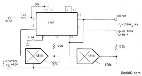
Two Optical Electronics S898 four-quadrant analog multipliers and 3704 state-variable active filter permit use of voltage control for changing filter characteristics remotely without having noise pickup problems on control Iines. Analog multipliers serve as variable-gain blocks that change cument levels in resistors and in effect change resistor values. Circuit has Iinear relationship of frequency to control voltage, constant gain andQwith frequency, and good temperature stability.- Voltage-Controll ed Active Bandpass Filter, Optical Electronics, Tucson, AZ, Application Tip 10269. (View)
View full Circuit Diagram | Comments | Reading(797)
Temperature_scanner
Published:2009/7/24 2:18:00 Author:Jessie
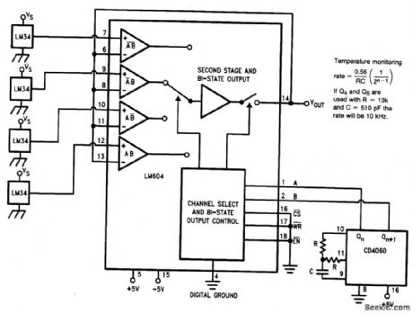
Fig. 13-13 This circuit uses an LM604 mux/amplifier to monitor several temperatures periodically, rather than continuously. Each channel is multiplexed to the output, according to the AB channel select. The CD4060 ripple binary counter has an on-board oscillator for continuous updating of the channel selects. National Semiconductor, Linear Applications Handbook 1991 p 1080. (View)
View full Circuit Diagram | Comments | Reading(770)
Indoor_outdoor_thermometer
Published:2009/7/24 2:14:00 Author:Jessie
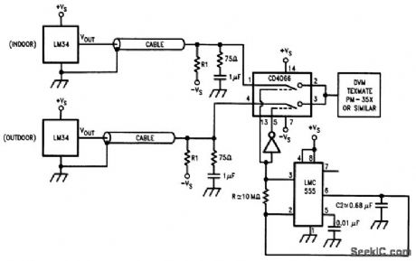
Pig. 13-10 The indoor and outdoor LM34 outputs are multiplexed through a CD4066 quad bilateral switch and then displayed (one at a time) on a DVM such as Texmate's PM-35X. Temperature range is -50° to +300°F. The LMC555 timer is run as an astable MV at 0.2 Hz so that each temperature is displayed for about 2.5 s. The RC filters at the LM34 outputs compensate for the capacitive loading of the cable. Notice that R1 must be selected to provide 50μA with the available -U supply (see Fig. 13-3). An LMC7660 can be used to provide -VS. National Semiconductor, Linear Applications Handbook, 1991, p. 1078. (View)
View full Circuit Diagram | Comments | Reading(1086)
Temperature_to_digital_converter_parallel_output
Published:2009/7/24 2:09:00 Author:Jessie
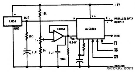
Fig. 13-7 This circuit converts temperature (from 0 to 128°F) to a parallel data word (8 bits when appropriate read, write, chip-select signals are received from the system). The circuit can be interfaced with a standard microprocessor data bus, and it provides an interrupt signal to the microprocessor. The scales are adjusted by the 1-kΩ pot so that all 8 bits are at digital1 when the temperature is +128°F. In practice, the VREF/2 pin of the ADC0804 is set to 0.64V. National Semiconductor Linear Applications Handbook. 1991 p 1077. (View)
View full Circuit Diagram | Comments | Reading(719)
Temperature_to_digital_converter_serial_output
Published:2009/7/24 2:07:00 Author:Jessie
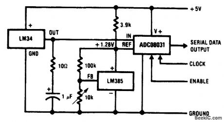
Fig. 13-6 This circuit converts temperature (from 0 to 128°F) to a serial data word (8 bits when appropriate clock and enable signals are received from the system). The scales are adjusted by the 10-kΩ pot so that all 8 bits are at digital 1 when the temperature is + 128°F, In practice, the VREF pin of the LM385 is set to 1.28 V. National Semiconductor, Linear Applications Handbook 1991 p 1076. (View)
View full Circuit Diagram | Comments | Reading(702)
Remote_temperature_sensor_output_referenced_to_ground
Published:2009/7/24 2:06:00 Author:Jessie

Fig. 13-5 This circuit is similar to that of Fig. 13-4, except that is not grounded and the output is referred to ground (slightly above ground). National Semicondutor Linear Applications Handbook 1991 p 1076. (View)
View full Circuit Diagram | Comments | Reading(586)
TRACKING_QUAD_GAIN_CONTROL
Published:2009/7/2 8:31:00 Author:May
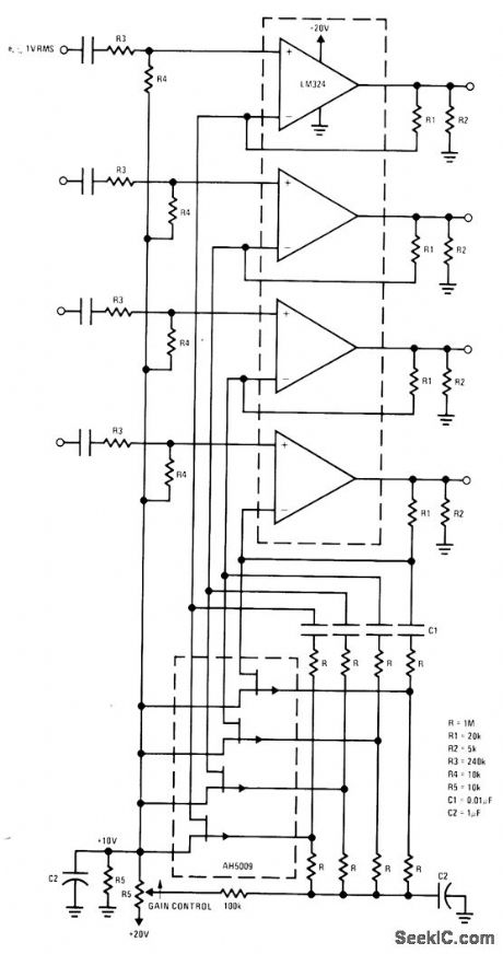
Basic circuit for each channel uses section of National LM324 quad opamp with section of AH5009 quad FET in feedback path. Each channel is AC coupled and has 40-dB range (gain range of 1 to 100).Bandwidth is minimum of 10 kHz. and S/N ratio is better than 70 dB with 4.3-VRMS maxi-mum output.-J. Sherwin, A Linear Multiple Gain-Controlled Amplifier. National Semiconductor. Santa Clara. CA. 1975. AN-129. p 6. (View)
View full Circuit Diagram | Comments | Reading(751)
Bar_graph_temperature_display_dot_mode
Published:2009/7/24 2:13:00 Author:Jessie
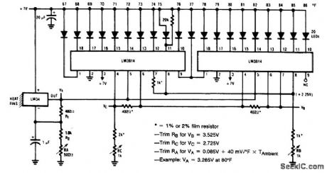
Fig. 13-9 This circuit combines an LM34 temperature sensor, two LM3914 display drivers, and 20 LEDs to form a temperature display where the temperature is indicated by turn-on of the corresponding LED (from 67 to 86°F). The temperature range can be increased by cascading several LM3419s. The display can be converted from the dot mode to the bar mode, or to flash a bar of LEDs when the temperature sensed reaches a selected limit. This requires a few extra components, as shown on the LM3419 datasheet. Note that the trim values for VA, VB and 1/C are for the temperature range show. UB and VC represent the highest and lowest temperatures, respectively. VA is set for gain of 4 (40 mV/°F instead of the nominal 10 mV/'F provided by the LM34). National Semiconductor Linear Applications Handbook 1991 p 1077. (View)
View full Circuit Diagram | Comments | Reading(5753)
TWO_STAGE_POSTAMPLIFIER
Published:2009/7/2 7:52:00 Author:May
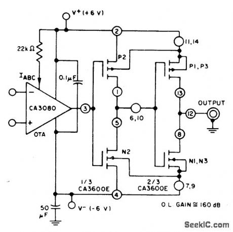
Connections shown for CA36OOE CMOS transistor-pair array give total open-loop gain of about 160 dB for system. Open-loop slew rate is about 65 V/μs.- Linear Integrated Circuits and MOS/FET's. RCA Solid State Division, Somerville, NJ, 1977, p278-279. (View)
View full Circuit Diagram | Comments | Reading(733)
Remote_temperature_to_frequency_converter
Published:2009/7/24 2:12:00 Author:Jessie
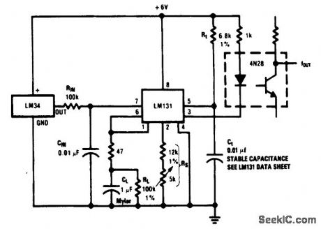
Fig. 13-8 This circuit converts temperature (from +3°to +300°F) to a corresponding frequency (30 to 3000 Hz). The output is isolated by a 4N28. The circuit can be used to send temperature information across long transmission lines because the 4N28 output voltage can be selected, as required. The scales are adjusted by the total value of RS (12-kΩ fixed and 5-kΩ variable). In practice, when RS is set to about 14.2 kΩ, the output is 10 Hz/°F. (View)
View full Circuit Diagram | Comments | Reading(1278)
| Pages:146/312 At 20141142143144145146147148149150151152153154155156157158159160Under 20 |
Circuit Categories
power supply circuit
Amplifier Circuit
Basic Circuit
LED and Light Circuit
Sensor Circuit
Signal Processing
Electrical Equipment Circuit
Control Circuit
Remote Control Circuit
A/D-D/A Converter Circuit
Audio Circuit
Measuring and Test Circuit
Communication Circuit
Computer-Related Circuit
555 Circuit
Automotive Circuit
Repairing Circuit