
Control Circuit
Index 158
Fast reverse amplifier with high input impedance circuit
Published:2011/7/28 4:17:00 Author:John | Keyword: Fast reverse amplifier, high input impedance
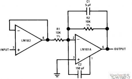
Fast reverse amplifier with high input impedance circuit is shown.
(View)
View full Circuit Diagram | Comments | Reading(729)
Traditional op-amp inverting attenuator circuit
Published:2011/7/28 4:16:00 Author:John | Keyword: op-amp, inverting attenuator
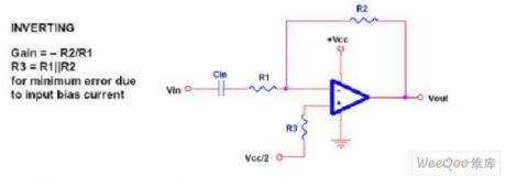
Traditional op-amp inverting attenuator circuit is shown.
(View)
View full Circuit Diagram | Comments | Reading(2401)
Addition and subtraction counter within 100 circuit
Published:2011/7/28 4:14:00 Author:John | Keyword: Addition and subtraction counter

Addition and subtraction counter within 100 circuit is shown.
(View)
View full Circuit Diagram | Comments | Reading(970)
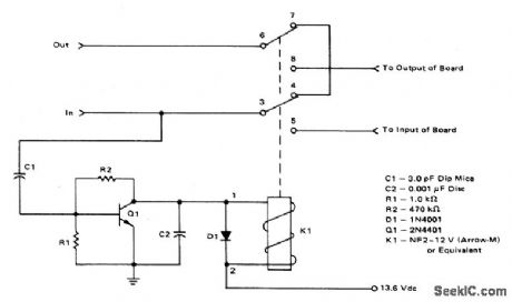
CARRIER_OPERATED_RELAY
Published:2009/6/29 4:00:00 Author:May
View full Circuit Diagram | Comments | Reading(6)
TONE_ACTUATED_RELAY
Published:2009/6/29 3:57:00 Author:May

The circuit is built around the LM567 tone decoder IC that requires about 100 millivolts at its operating frequency. The frequency is set by a 10 K variable resistor and can be between 700 and 1500 Hz. When a tone at the set fre-quency is present, the 567's output goes low to energize a relay through a 2N3906 PNP transistor. (View)
View full Circuit Diagram | Comments | Reading(2519)
ONE_PULSE_PER_PUSH
Published:2009/6/29 3:47:00 Author:May
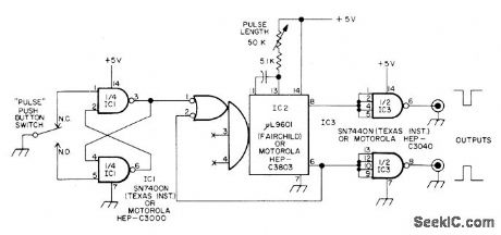
Circuit generates only one rectangular pulse for each actuation of pushbutton switch, even if contacts bounce.TTL gates IC1 are wired as RS flip-flop (latch) that triggers mono MVBR IC2 having fixed-duration positive and negative output pulses.Output drives are increased by TTL inverting buffer gates.—H. Olson, Further Adventures of the Bounceless Switch, 73 Magazine, Feb. 1975, p 111-114. (View)
View full Circuit Diagram | Comments | Reading(1284)
REMOTE_ON_OFF_SWITCH
Published:2009/6/29 3:47:00 Author:May
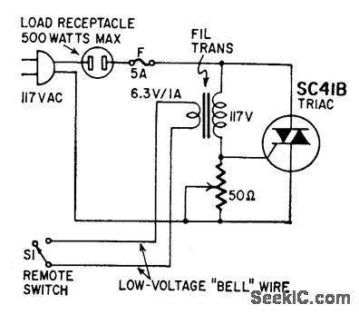
This circuit provides power control with-out running line-voltage switch leads. The primary of a 6-volt filament transformer is con-nected between the gate and one of the main terminals of a triac. The secondary is connected to the remote switch through ordinary low-voltage line. With switch open, transformer blocks gate current, prevents the triac from firing and applying power to the equipment. Closingthe switchshort-circuits the secondary, causing the transformer to saturate and trigger the triac. (View)
View full Circuit Diagram | Comments | Reading(1190)
Precision_current_sink
Published:2009/7/24 22:41:00 Author:Jessie
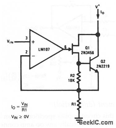
As shown,the ability of this circuit to sink current depends on VIN and the value of R1. Note that VIN can be anything from 0 to (V+-1V), and can be +2 to +25 V. (View)
View full Circuit Diagram | Comments | Reading(1)
Op_amp_offset_adjustment_inverting
Published:2009/7/24 22:39:00 Author:Jessie
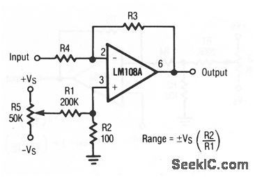
Although this circuit applies specifically to an LM108A, the values and equations can be adapted to virtually any op amp connected in the inverting configuration. (View)
View full Circuit Diagram | Comments | Reading(721)
Op_amp_offset_adjustment_differential
Published:2009/7/24 22:20:00 Author:Jessie
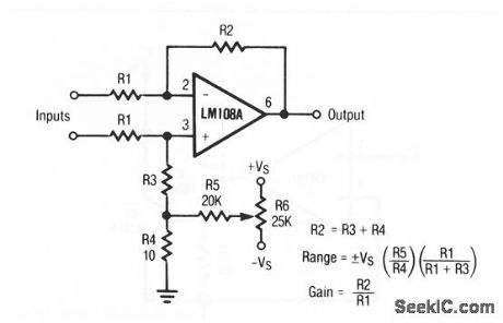
Although this circuit applies specifically to an LM108A, the values and equations can be adapted to virtually any op amp connected in the differential-input configuration. (View)
View full Circuit Diagram | Comments | Reading(1524)
Op_amp_offset_adjustment_noninverting
Published:2009/7/24 22:19:00 Author:Jessie
Although this circuit applies specifically to an LM108A, the valuesand equations can be adapted to virtually any op amp connected In the noninverting configuration. (View)
View full Circuit Diagram | Comments | Reading(807)
SWITCH_CLOSURE_COU_NTER
Published:2009/6/29 2:40:00 Author:May
National MM5865 universal timer and counter chip is used with 74C00 debouncer and LM555C timer to drive digital display that counts closures of manual switch S3. Reset transition restores display to 0000. BCD segment outputs of MM5865 feed LED 4-digit display through MM14511 interface, whiledigit enable outputs go to display through DM8863 driver.— MOS/LSI Databook, National Semiconductor, Santa Clara, CA, 1977, p 2-23-2-32. (View)
View full Circuit Diagram | Comments | Reading(862)
Digitally_controlled_threshold_detector
Published:2009/7/24 22:16:00 Author:Jessie
Figure 6-47 shows a MAX941 comparator combined with a MAX512 DAC to form a digitally controlled threshold detector. The analog signal to be compared is applied directly to the inverting input of the MAX941. The threshold point is set by the DAC output applied to the noninverting input. In turn, the DAC output is set by the serial digital input. As a result, the threshold can be set in eight discrete steps (depending on the serial input). MAXIM NEW RELEASES DATA BOOK, 1995, P. 3-69. (View)
View full Circuit Diagram | Comments | Reading(822)
SIMPLE_TIME_DELAY
Published:2009/6/29 2:40:00 Author:May
View full Circuit Diagram | Comments | Reading(0)
TIMER
Published:2009/6/29 2:39:00 Author:May
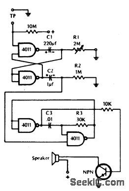
The timer can be used wherever time periods of up to seven minutes duration are needed. To turn on just touch the turn-on plate, and after the selected time has elapsed, an alarm will sound for a short period, then au-tomatically turn off. The turn-on touch plate, labeled TP in the diagram, is made up of two metal strips about 1/16-inch apart. Bridging the gap with your finger activates the timer. For more time range, increase RI and/or C1. R2 and C2 determine the period of time that the alarm will sound. Increasing either will extend the time. The tone of the alarm is determined by R3 and C3. Increasing either lowers the tone, decrqasing them raises the tone. (View)
View full Circuit Diagram | Comments | Reading(1093)
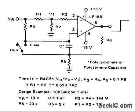
741_TIMER
Published:2009/6/29 2:37:00 Author:May
R1 and R2 hold the inverting input at half supply voltage. R4 applies feedback to increase the input impedance at pin 3. Pin 3, the nonin-verting input, is connected to the junction of R3 and C. Afterthe switch is opened, C charges via R3. When the capacitor has charged sufficiently for the potential at pin 3 to exceed that at pin 2 the output abruptly changes from 0 V to positive line potential. If reverse polarity operation is required, simply transpose R3 and C. R3 and C can be any values. Time delays from a frac-tion of a second to several hours can be ob-tained by judicious selection. The time delay-independent of supply voltage-is 0.7CR seconds where C is in farads. (View)
View full Circuit Diagram | Comments | Reading(1872)
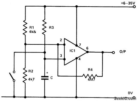
LONG_INTERVAL_RC_TIMER
Published:2009/6/29 2:35:00 Author:May
View full Circuit Diagram | Comments | Reading(729)
SIMPLE_TIMER
Published:2009/6/29 2:33:00 Author:May
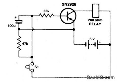
Press S1. The 100 μF electrolytic capacitor rapidly charges up at about 0.7 V. The transistor will be forward biased, and collector current will flow operating the relay. Release S1. The capacitor will begin to discharge via the 33 K resistor at the base of the transistor. When the voltage across the capacitor gets down to half a volt or so, the transistor base will no longer be forward biased, collector current will cease, and the relay will drop out. The capacitor will continue to discharge via the 47 K resistor. With the values shown, the relay will remain operated for about eight seconds. Long times are possible with lower values of capacitance by substituting a Darlington pair for the 2N2926. In this case, increase the two resitor values into the megohm range. (View)
View full Circuit Diagram | Comments | Reading(925)
TIMING_CIRCUIT
Published:2009/6/29 2:31:00 Author:May
Load current starts approximately 0.5 RC after the switch IS thrown. (View)
View full Circuit Diagram | Comments | Reading(0)
ON_OFF_CONTROLLER
Published:2009/6/29 2:31:00 Author:May
The ac line-operated on/off controller is a simple, reliable solid-state altemative to a mo-tive driven cam switch. Time 1 and time 2 are programmed by diodes to be 8 hours and 20 hours respectively. The TIM1 output is buffered by a transistor to supply gate current to a triac which switches the output load. When power is applied to the circuit, the output load is switched on for 8 hours then off for 20 hours repeatedly. (View)
View full Circuit Diagram | Comments | Reading(1000)
| Pages:158/312 At 20141142143144145146147148149150151152153154155156157158159160Under 20 |
Circuit Categories
power supply circuit
Amplifier Circuit
Basic Circuit
LED and Light Circuit
Sensor Circuit
Signal Processing
Electrical Equipment Circuit
Control Circuit
Remote Control Circuit
A/D-D/A Converter Circuit
Audio Circuit
Measuring and Test Circuit
Communication Circuit
Computer-Related Circuit
555 Circuit
Automotive Circuit
Repairing Circuit