
Control Circuit
Index 145
SLOW_SWEEP_WIPER_CONTROL
Published:2009/7/3 3:19:00 Author:May
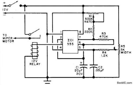
The relay which applies power to the wiper motor is actuated at periodic intervals by the timer circuit, closing the wiper motor contacts.R5 Potentiometer R1 serves as the pulse rate control and potentiometer R5 as the pulse width control. These two controls should be adjusted for optimum performance after the unit is installed in a car. (View)
View full Circuit Diagram | Comments | Reading(1411)
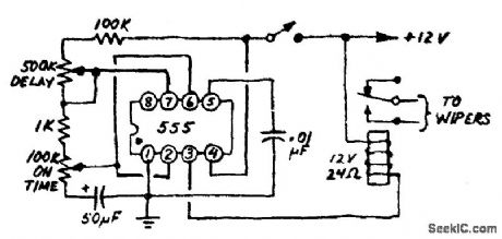
DELAYED_ACTION_WINDSHIELD_WIPER_CONTROL
Published:2009/7/3 3:17:00 Author:May
View full Circuit Diagram | Comments | Reading(687)
DC_MOTOR_SPEED_CONTROL
Published:2009/7/3 3:11:00 Author:May
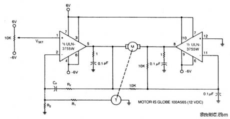
Power op amps provide accurate speed control for dc motors. The circuit provides bidirectional speed control. The amplifiers' push-pull configuration ensures a full rail-to-rail voltage swing (minus the output stages' saturation drops) across the motor in either direction. The circuit uses a mechanically-coupled tachometer to provide speed-stabilizing feedback to the first amplifier section. The motor's speed and direction of rotation is set by adjusting the 10 k ohm potentiometer at the amplifier's noninverting input. The RFCF feedback network prevents oscillation by compensating for the inherent dynamic mechanical lag of the motor. Select the RFCF time constant to match the particular motor's characteristics. (View)
View full Circuit Diagram | Comments | Reading(0)
BACK_EMF_PM_MOTOR_SPEED_CONTROL
Published:2009/7/3 3:09:00 Author:May
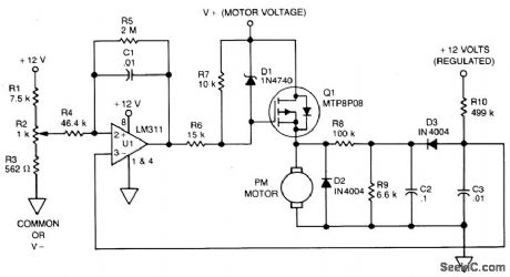
The use of power MOSFETs allows a direct interface between logic and motor power, which permits circuit simplicity as well as high efficiency. This speed control circuit can be packaged on a 22-pin, double-sided, 3.5 x 4-in. pc board.
A 12 V control supply and a TRW BL11, 30V motor are used; with minor changes other motor and control voltages can be accommodated. For example, a single 24V rail could supply both control and motor voltages. Motor and control voltages are kept separate here because CMOS logic is used to start, stop, reverse and oscillate the motor with a variable delay between motor reversals.
Motor speed is established by potentiometer R2, which applies a corresponding dc voltage to the + input of comparator U1, whose output is then applied to TMOS device MTP8P08 (Q1). Zener diode D1 limits the drive to Q1. The output of Q1 drives the permanent magnet motor.
Back emf is obtained from the motor via the network consisting of R8, R9, R10, C2, C3 and D3; it is applied to-input of comparator U1. (View)
View full Circuit Diagram | Comments | Reading(1994)
OVERVOLTAGE_PROTECTION_CIRCUIT_SCR_CROWBAR
Published:2009/7/3 3:08:00 Author:May
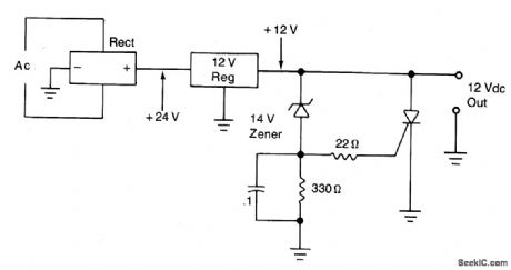
Circuit Notes
The silicon controllqd rectifier (SCR) is rated to handle at least the current of the power supply. It is connected in parallel across the 12 V dc output lines, but remains inert until a voltage appears at the gate terminal. This triggering voltage is supplied by the zener diode. At potentials less than 14 V the zener will not conduct current. But, at potentials greater than 14 Vdc the zener conducts and creates a voltage drop across the 330 ohm resistor that will fire the SCR. When the SCR turns on, the output lines of the power supply are shorted to ground. This will blow the primary fuse or bum out the transformer if there is no primary fuse. (View)
View full Circuit Diagram | Comments | Reading(2202)
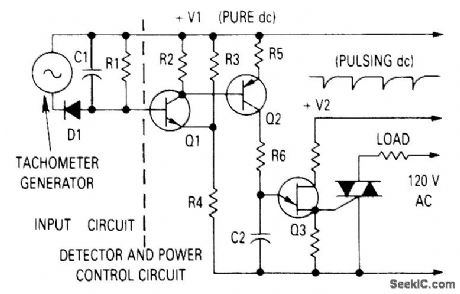
CONSTANT_SPEED_MOTOR_CONTROL_USING_TACHOMETER_FEEDBACK_
Published:2009/7/3 3:07:00 Author:May
The generator output is rectified then filtered and applied between the positive supply voltage and the base of the detector transistor. This provides a negative voltage which reduces the base-voltage when the speed increases. In normal operation, if the tachometer voltage is less than desired, the detector transistor is turned on, then turns on Q2 which causes the timing capacitor for the unijunction transistor to charge quickly. As the tachometer output approaches the voltage desired, the base-emitter voltage is reduced to the point at which Q1 is almost cut off. Thereby, the collector current which charges the unijunction timing capacitor is reduced, causing that capacitor to charge slowly and trigger the thyristor later in the half cycle. In this manner, the average power to the motor is reduced until just enough power to maintain the desired motor speed is allowed to flow. (View)
View full Circuit Diagram | Comments | Reading(691)
MOTOR_SPEED_CONTROL_CIRCUIT
Published:2009/7/3 3:07:00 Author:May
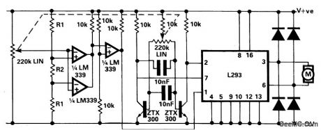
A shortcoming of the above bi-directional proportional motor control circuit is that with the potentiometer in its center position the motor does not stop, but creeps due to the difficulty in setting the potentiometer for an exact 1:1 mark-space ratio from the flip-flop. This modified circuit uses a second potentiometer, ganged with the first used to inhibit drive to the motor near the center position. This potentiometer is connected between the supply lines and feeds a window comparator which in turn drives the inhibit input of the L293. (View)
View full Circuit Diagram | Comments | Reading(1175)
PWM_MOTOR_SPEED_CONTROL
Published:2009/7/3 3:03:00 Author:May
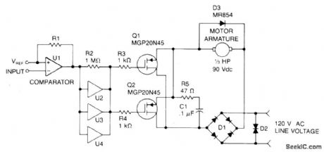
Speed control is accomplished by pulse width modulating the gates of two MGP20N45 TMOS devices. Therefore, motor speed is proportional to the pulse width of the incoming digital signal, which can be generated by a microprocessor or digital logic.The incoming signal is applied to comparator U1, then to paralleled inverters U2, U3, and U4 that drive the two TMOS devices, which, in turn, control power applied to the motor armature. Bridge rectifier Dl supplies fullwave power that is filtered by R5 and C1. Free-wheeling diode D3 (MR854) prevents high voltage across Q1 and Q2.A back-to-back zener diode, D2, protects against transients and high voltage surges. (View)
View full Circuit Diagram | Comments | Reading(1241)
BI_DIRECTIONAL_PROPORTIONAL_MOTOR_CONTROL
Published:2009/7/3 3:01:00 Author:May
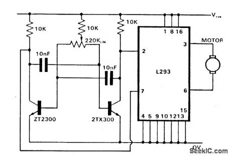
The control of both direction and of proportional motor speed is achieved by rotation of a single potentiometer. The motor driver is an SGS integrated circuit L293 which will drive up to 1 amp in either direction, depending on the logic state of input 1 and input 2 as per table.
I/P1 I/P2 FunctionHigh Low Motor turns one way Low High Motor reverses
By applying a variable M/S ratio flip-flop to these inputs, both speed and direction will be controlled. With RV1 in its center position the M/S will be 1:1 whereby the motor will remain stationary due to its inability to track at the flip-flop frequency. Movement of RV1 in either direction will gradually alter the M/S ratio and provide an average volt-age bias in one direction proportional to the M/S ratio. (View)
View full Circuit Diagram | Comments | Reading(2288)
CARRIER_OPERATED_RELAY_
Published:2009/7/3 3:00:00 Author:May
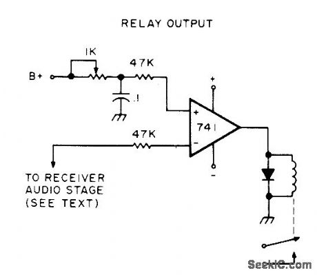
Relay is energized when carrier is present in FM receiver, to activate transmitter for repeater applications or turn on tape recorders, alarms, or other devices.Will work with either solid-state or tube-type receivers. Inverting (minus) input of opamp is connected directly to collector of audio preamp transistor or any other point having voltage change between signal and nosignal. If voltage change is in wrong direction, reverse leads to opamp input. Use 1K pot to set reference voltage so relay trips reliably on incoming signal.Relay can be reed-type drawing less than 75 mA.-S. Uhrig, The 5 Minute C0R, 73 Magazine, Dec. 1976, p 152-153. (View)
View full Circuit Diagram | Comments | Reading(3413)
BURGLAR_ALARM_2
Published:2009/7/3 3:00:00 Author:May
This circuit cannot be shut off for 10 to 60 seconds-even if the trip condition is immediately removed.It draws no standby power from the battery and is self-resetting.
(View)
View full Circuit Diagram | Comments | Reading(679)
BURGLAR_ALARM
Published:2009/7/3 2:58:00 Author:May
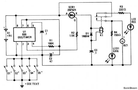
The heart of the circuit is a 555 oscillator/timer, U1, configured for monostable operation. The output of U1 at pin 3 is tied to the gate of SCR1. As long as S1-S5, which are connected to the trigger input of U1, are open, the circuit remains in the ready state, and does not trigger SCR1 into conduction. Because the relay is not energized, battery current is routed through the relay's normally-closed terminal and through current-limiting resistor R3 to LED2, causing it to light.However, when one of the switches (S1-S5) is closed, grounding U1 pin2, the output of U1 at pin 3 increases, activating SCR1. That energizes the relay, pulling the wiper of K1 to the normally-open termi-nal, causing LED1 to light and BZ1 to sound.The duration of the output is determined by the RC time-constant circuit, formed by R1 and C1.Resistor R2 regulates the output of U1 to a safe value for the gate of SCR1. Switches S1-S5 are to doors, windows, etc. A switch can be connected in series with B1 to activate and deactivate the alarm circuit when it's not needed. (View)
View full Circuit Diagram | Comments | Reading(0)
LOW_VOLTS_ALARM
Published:2009/7/3 2:55:00 Author:May
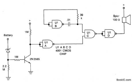
Circuit Notes
This inexpensive dc supply-voltage monitor sounds a warning when the voltage falls below a preset value. It is ideal for monitoring rechargeable batteries since it draws only a few microamperes when not sounding. The voltage at which the alarm sounds is determined by the zener diode. When the voltage falls below the zener voltage, the alarm sounds. The alarm tone is determined by the RC time constant of the 39 k resistor and 0.01 mf capacitor. (View)
View full Circuit Diagram | Comments | Reading(1024)
FSK_OSCILLATOR_FOR_EKG_RELAY
Published:2009/7/3 2:49:00 Author:May
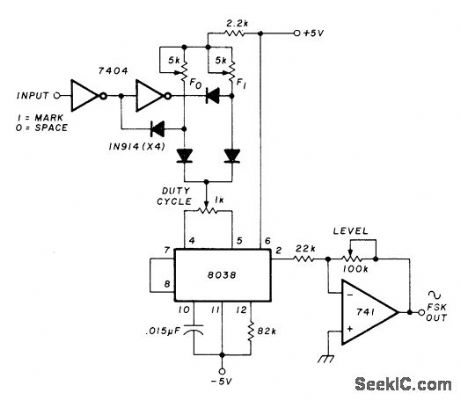
Used in satellite system for relaying electrocardiograms in digital form. Input consists of 8-bit words obtained in serial form from universal asynchronous receiver-transmitter. Uses 8038 function generator that is switched between two adjustable trimmer resistors giving independently ad justable discrete audio frequencies for mark and space. Output is phase-coherent even though switching does not necessarily take place at zero-crossing points of sine wave. 0peration is much like that of FSK RTTY.-D. Nelson, Medical Lbata Relay via Oscar Satellite, Ham Radio, April 1977, p 67-73. (View)
View full Circuit Diagram | Comments | Reading(1598)
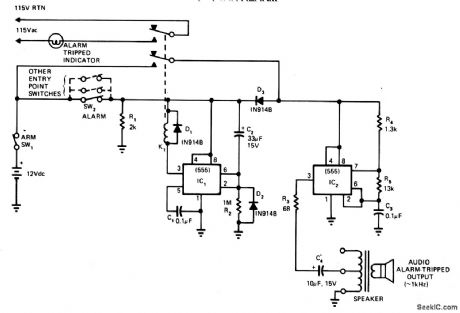
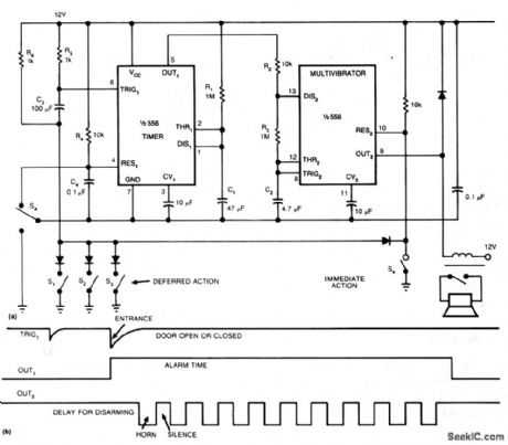
SINGLE_IC_AUTO_ALARM
Published:2009/7/3 2:36:00 Author:May

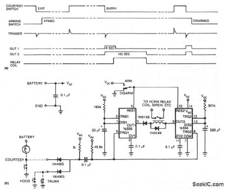
See (a) for the timing information for the alarm circuit in (b). When leaving your vehicle, flip the arming switch and close the door to arm the device. Subsequent opening of an entrance triggers both timers.After the expiration of the entry delay timer, the alarm sounds for a time determined by the second timer.The value of R should be less than 1 KΩ. If you use an incandescent lamp instead of a resistor, you get an extra function-an open-entrance indicator. By keeping the resistance low, you avoid false tripping should water collect under the hood. If your door switch connects the courtesy light to 12 V rather than ground, use a single transistor as an inverter at the input. (View)
View full Circuit Diagram | Comments | Reading(844)
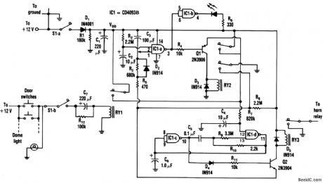
SEMICONDUCTOR_FAIL-SAFE_ALARM
Published:2009/7/3 2:32:00 Author:May

False alarms produced by semiconductor failure are impossible with this burglar-alarm circuit equipped with relays. What's more, the circuit is virtually immune to false triggering. With a standby current of less than 0.1 mA, the circuit offers all the features an alarm needs: entry and exit delays, a timed alarm period, and automatic reset after an intrusion.One CMOS CD4093B quad NAND gate, IC1, supplies both logic and analog timing functions with the aid of Schmitt-trigger switching action. Relays make the circuit fail-safe in the alarm-active mode, even when the semiconductors fail. The relays are 12-V, with coil resistances of 250 Ω or more.Closing switch S1 initiates circuit operation. Capacitor C2 begins charging through resistor R2 and arming indicator LED1 lights. When pin 2 of ICla reaches its switching point, its output decreases, extinguishing LED1 and indicating that the exit delay has ended. That output also drives the base of Q1 low, so that if the emitter circuit completes to the VDD line, Q1 conducts. The circuit is now armed, and current drain drops to less than 0.1 mA.When the vehicle is entered, relay RY1 contacts close momentarily, completing the emitter circuit of Q1 and causing the RY2 contacts to close. Charging C4 through R7 determines the entry-delay period. If the system isn't turned off by opening S1 during this period, the oscillator circuit of IClc and ICld activates, and a rapid on/off horn-honking cycle kicks on with the aid of Q2 and RY3.The alarm cycle ends after about a minute, when C2 charges through R3 to the threshold voltage of ICla at pin 1. This voltage resets the timing circuit, readying it for another entry/alarm cycle. RY1 is connected for vehicles that use door switches connected to +12 V. For vehicles that use grounding door switches, the bottom of the RY1 coil should connect to + 12 V instead of ground. In the latter case, the polarity of C7 should be reversed. 'For home use, the R3C3 time constant should be increased to give a longer alarm. (View)
View full Circuit Diagram | Comments | Reading(1165)
FORCED_SWITCHING
Published:2009/7/24 4:03:00 Author:Jessie
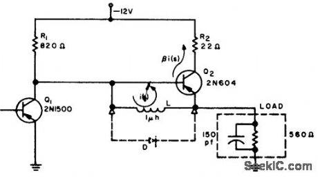
Bypassing of emitter-follower with inductor L cuts normal 70-nsec switching time to 38 nsec. Use of diode D across L improves rise time without affecting fall lime.-T. Asai, Forced-Switching Emitter Follower, EEE, 12:2, p 29. (View)
View full Circuit Diagram | Comments | Reading(680)
ONE_CHIP_BURGLAR_ALARM
Published:2009/7/3 2:27:00 Author:May
The single-chip, burglar-alarm circuit shown uses a dual 556 timer, draws 10 mA of standby current, and generates a pulsing alarm signal that conserves battery energy. Once activated, the alarm will remain on, independent of the subsequent state of any of the sensors. The sensors support both deferred and immediate-action modes. You can attach this circuit to your car's internal lighting circuitry using a single wire and a relay. To arm this circuit, you open your car door and close switch SA. The switch discharges capacitor C4 and holds the timer (one half of the 556 IC) in a reset state to prevent false triggering while you're arming the circuit. When you close your car door, the circuit enters a standby mode. If the door is then reopened, the sensors apply a negative-going pulse to trigger 1. Output 1 then increases, enabling the alarm for 1.1RlC1 seconds. Output 1's high state triggers the multivibrator, the other half of the 556, which begins to cycle after a delay equal to 1.1 (R2 + R3) C2 seconds. As long as the timer's output stays high, the multivibrator will continue to cycle, turning the horn off and on at 3.3-second intervals. During the interval between time that the timer's output increases and the time that the multivibrator's output decreases, you can disarm this circuit using switch SA. To prevent false triggering caused by switch contacts, at S1, S2, and S3, that may bounce when closing the door, make the R6C3 time constant as large as possible. In addition, capacitors C1 and C2 should be tantalum types and should exhibit leakage of less than 1 μA at room temperature.
(View)
View full Circuit Diagram | Comments | Reading(2169)
FAST_ACTION_AT_10_KC
Published:2009/7/24 4:03:00 Author:Jessie
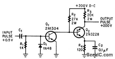
Reverse bias is applied to gate of scr at cutoff to make switch open rapidly. Rise time is 10 microsec and fall time 5 microsec for switching 10 ma at up to 10 kc.-E. L. Dosch, SCR Switch Turns Off With Reverse Bias, Electronics, 38:7, p 88. (View)
View full Circuit Diagram | Comments | Reading(654)
AUTO_ALARM
Published:2009/7/3 2:25:00 Author:May
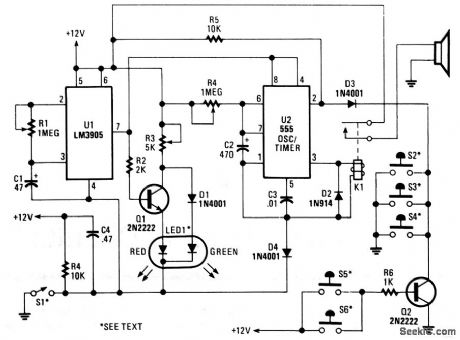
In operation, the alarm circuit allows a 0-47 second time delay, as determined by the R1/C1 combination, after the switch is armed to allow the vehicle's motion sensor to settle down. This allows you time to get a bag of groceries out of the trunk and not have the hassle of juggling the groceries and the key switch at once.During the time delay, half of LED1, which is actually a single, bi-colored, three-legged common cathode device, lights green. At the same time, pins 8 and 4 of U2 (a 555 oscillator/timer) are held low by U1 (a 3905 oscillator/timer), causing the alarm to remain silent. Once the delay is over, LED1 turns red, indicating that the circuit is armed.At that point, a ground at pin 2 of U2 forces pin 3 of U2 high, closing the contacts of K1 and sounding the siren for a time duration determined by R4 and C2. Once the time has elapsed, pin 3 is pulled low, K1 opens, and the circuit is again ready to go. The circuit can be manually reset by the simple expedient of opening and closing the key switch. Potentiometer R3 controls the LED's illumination intensity. Diode Dl ensures that the green segment of LED1 is fully extinguished when Q1 is turned on-which turns the LED to red. Resistors R4 and R5 must be connected to the +V bus, not to pin 7 of U1, otherwise U2 will mysteriously trigger itself each time the initial delay ends. (View)
View full Circuit Diagram | Comments | Reading(1)
| Pages:145/312 At 20141142143144145146147148149150151152153154155156157158159160Under 20 |
Circuit Categories
power supply circuit
Amplifier Circuit
Basic Circuit
LED and Light Circuit
Sensor Circuit
Signal Processing
Electrical Equipment Circuit
Control Circuit
Remote Control Circuit
A/D-D/A Converter Circuit
Audio Circuit
Measuring and Test Circuit
Communication Circuit
Computer-Related Circuit
555 Circuit
Automotive Circuit
Repairing Circuit