
Control Circuit
Index 144
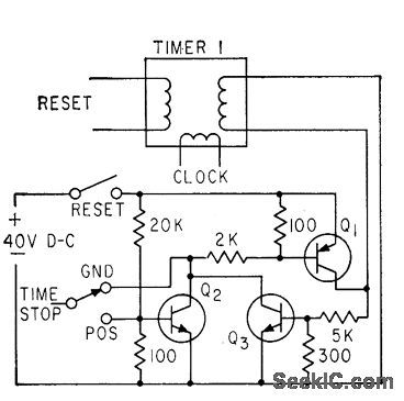
START_STOP_CONTROL
Published:2009/7/23 22:22:00 Author:Jessie
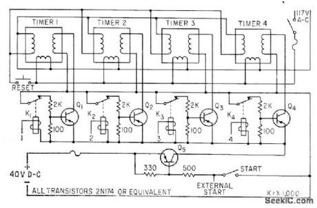
Low-cost transistor arrangement controls four precision timers used for simultaneous measurement of lime interval of four integrating circuits. Time between first digital output pulse and firing of circuit is determinable within 0.01%.-F. W. Kear, Tests Show Control is Key to Timer Accuracy, Electronics, 33:27, p 62. (View)
View full Circuit Diagram | Comments | Reading(1041)
Serial_controlled_8_channel_SPST_switch_MAX335
Published:2009/7/23 22:22:00 Author:Jessie
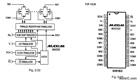
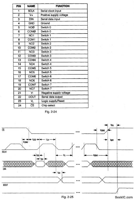
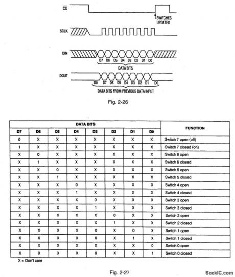
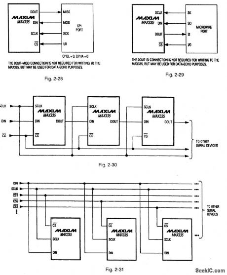
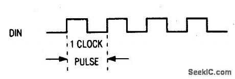
Figures 2-22, 2-23 and 2-24 show the functional diagram, pin configuration, and pin description, respect-tively, for the MAX335.Figures 2-25 and 2-26 show the timing, and three-wire interface timing, respectively. Figure 2-27 shows the serial-interface switch programmlng.This IC has eight separately controlled single-pole-single-throw(SPST) switches, all of which conduct equally in either direction, with an on-resistance(100Ω) that is constant over the analog signal range. The switches can continuously operate with supplies from ±4.5 V to ±20 V, and handle rail-to-rail analog signals. Upon power-up, all switches are off, and the internal serial and parallel shift registers are reset to zero. The IC is equivalent to two DG211 quad switches, but controlled by a serial interface. The interface is compatible with both Motorola SPI(Fig.2-28) and Microwire (Fig.2-2),Functioning as a shift register,this serial interface allows data (at DIN) to be clocked In sync with the rising edge of clock (SCLK). The shift register output ( DOUT) enables several MAX335 ICs to be daisy-chained (Fig.2-30), or the ICs can be connected as an addressable serial interface (Fig.2-31) Digital - feedthrough transients are typically 10 mV p-p when a 100-pF capacitance is used at the switch channels.MAXIM NEW RELEASES DATA Book、1995, P. 1-59, 1-64, 1-65, 1-66, 1-67, AND 1-68. (View)
View full Circuit Diagram | Comments | Reading(1010)
RECYCLING_WITH_VARIABLE_DUTY_CYCLE
Published:2009/7/23 22:34:00 Author:Jessie
Two 100K variable resistors control on and off times. Gives time delays from 0.3 to 6 sec.-P. Gheorghiu, Recycling Timing with Variable Duty-Cycle, EEE, 13:4, p 41. (View)
View full Circuit Diagram | Comments | Reading(876)
Signal_line_circuit_protectors_fault_protected_switches
Published:2009/7/23 22:28:00 Author:Jessie

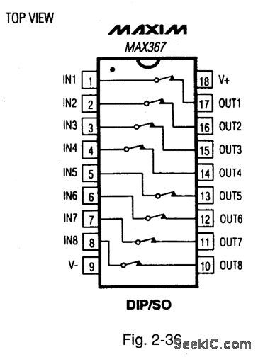
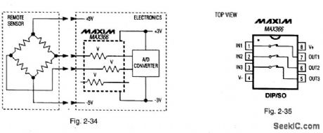
Figures 2-34 and 2-35 show a typical application circuit and pin configuration, respectively, for the MAX366. Pin configurations for the MAX337 are shown in Fig.2-36. These ICs are multiple, two-terminal circuit protectors. Placed in series with signal lines, each two-terminal device protects sensitive circuit components from damaging voltage near and beyond the normal supply range. The ICs are used at interfaces where sensitive circuits connect to the external world, and potentially damaging voltage (up to 135 V beyond the supply rails) might be encountered during power-up, power-down, or fault conditions. The ICs can be used to protect either analog or digital signals using unipolar (5 V to 44 V) or bipolar (±5 V to±22 V) supplies. The ICs are essentially fault-protected switches that are always on when power is applied. On resistance is 100Ω (max.), and leakage is less than 1nA at +25℃. When signal voltages exceed, or are within 1.5 V of the supply voltages, or when power, is off, the two-terminal resistance increases and becomes a virtual open circuit. This ensures low current during fault conditions. The protected side of the switch maintains the correct polarity and clamps about 1.5 V below the supply rail. There are no glitches or polarity reversals going into or coming out of a fault condition. ESD (electrostatic discharge) protection is greater than 2 kV.MAXIM NEW RELEASES DATA Book, 1995, P. 1-109, 1-110. (View)
View full Circuit Diagram | Comments | Reading(984)
UJT_TIMER
Published:2009/7/23 22:26:00 Author:Jessie
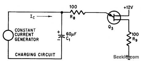
Charging current of C1 should be greater than 2Gmicroamp peak-point current at which Q3 is triggered and less thon 8-ma sustaining current of Q3, so ujt will turn off after it is triggered. 2N2422A may be used for Q3.-A. A. Lampell, Off-the-Shelf Integrated Circuits for Versatile and Accurato Timer, Electronics, 38:25, p 70-73. (View)
View full Circuit Diagram | Comments | Reading(826)
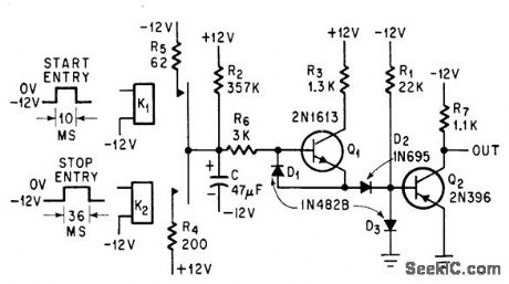
DUAL_POLARITY_START_STOP_CONTROL
Published:2009/7/23 22:40:00 Author:Jessie
Switches connect relay coils either to positive bus or to ground, so timer can be controlled by either positive or negative pulses. Additional transistor, used in place of relay, pro vides stop switching.Q3 forms damping cir. cult for use where stop pulse duration is too short.-F. W. Kear, Tests Show Control is Key to Timer Accuracy, Electronics, 33:27, p 62. (View)
View full Circuit Diagram | Comments | Reading(744)
TV_REMOTE_CONTROL_TESTER
Published:2009/7/23 22:39:00 Author:Jessie
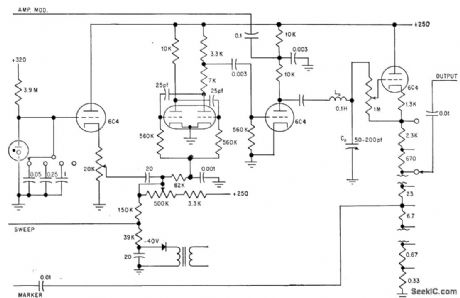
Grid-controlled mvbr has sweep of 0 to 7 kc, with center frequency adjustable from 36 to 44 kc. Maximum output is 85 v peak-to-peak. Neontube sweep generator operates at 1, 6, and 22 cps. Used for testing ultrasonic remote controls.-G. Row, Sweep Generator Tests Ultrasonic Remote Controls, Electronics, 34:47, p 64-66.
(View)
View full Circuit Diagram | Comments | Reading(694)
ENCODER_COUNTER
Published:2009/7/23 22:43:00 Author:Jessie
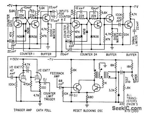
Counter, limit trigger, and blocking oscillator ore given for encoder used for storing and reading out elapsed time between consecutive randomly occurring events. First 23 counters are identical.-R. J. Kelso and J. C. Groce, Encoder Measures Random Event Time Intervals, Electronics, 32:12, p 48-51. (View)
View full Circuit Diagram | Comments | Reading(1148)
SING_AROUND_COUNTER_CONTROL
Published:2009/7/23 22:42:00 Author:Jessie
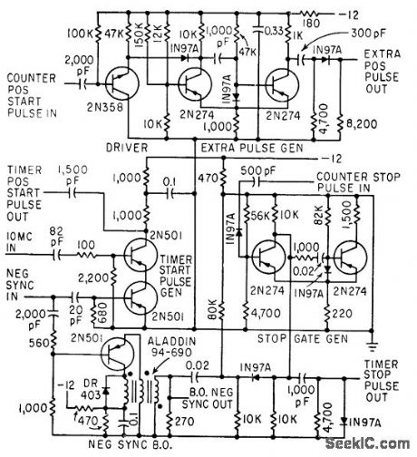
Timer start-pulse generator is fast series-transistor coincidence circuit. Slop-gate generator is one-shot mvbr that prevents 1N97A diode from passing blocking oscillator negative sync pulse until mvbr fires. Used to count number of sing-around cycles and measure total time in system for measuring ultrasonic velocity in liquids and solids.-R. L. Forgacs, Precision Ultrasonic Velocity Measurements, Electronics, 33:47, p 98-100. (View)
View full Circuit Diagram | Comments | Reading(687)
13_SEC_TIMER
Published:2009/7/23 22:42:00 Author:Jessie
Two silicon transistors start timing action when 10-millisec start pulse closes reed relay K1, making output transistor Q1 conductive for 13 sec. Timing period can be shortened by applying 36-millisec pulse to K2.-H. W. Hines and L. C. Radzik, Electronic Timer Provides Long Delay, Electronics, 37:17, p 63. (View)
View full Circuit Diagram | Comments | Reading(770)
SPDT_switches_MAX335
Published:2009/7/23 22:26:00 Author:Jessie
To use the MAX as a single-pole double-throw (SPDT) switch, tie COM0 to N01 so that N00 and COM1 are now inputs and COM0/N01 is the common output. Up to four SPDT switches can be made from each MAX335. Multiples of four or more can be made by daisy-chaining the ICs. Figure 2-33 shows the serial input control for SPDT switch operation. Again, CS is held low to clock in pulses, and pulled high to update; CS is also held low to shift pulses, then pulled high to update, etc. (View)
View full Circuit Diagram | Comments | Reading(680)
CURRENT_MODE_SWITCH
Published:2009/7/23 22:39:00 Author:Jessie

With l,000-Mc lime base applied to base of Q2, two current. mode switches together serve to give ac curacy of 0.5 nsec in measurement of time intervals with quinary scaler.-R. Englemann, Quinary Scalers: Measure Time Intervals Digitally, Electronics, 37:5, p 34-36. (View)
View full Circuit Diagram | Comments | Reading(744)
INTERVAL_TIMER
Published:2009/7/23 22:38:00 Author:Jessie
Interval is determined by C, which can be paralleled capacitors to in. crease range.-N. C. Hekimian, PNP-NPN CIRCUITS; New Look at a Familiar Connection, Electronics, 35:47, p 42-46. (View)
View full Circuit Diagram | Comments | Reading(702)
CLUTCH_COIL_FOR_TIMER_MOTOR
Published:2009/7/23 22:38:00 Author:Jessie
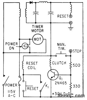
Start-and-stop signals are applied to stop jack, for automatic timing. Manual-timing pushbutton applies 0-v signal to stop jock, to make Q1 conduct. Fast switching rime of transistor permits reading time to within 0.005 millisec.-F. W. Kear, Electromechanical Timer for Lab Applications, Electronics, 36:7, p 78-79. (View)
View full Circuit Diagram | Comments | Reading(762)
400_CPS_DRIVER
Published:2009/7/23 23:26:00 Author:Jessie
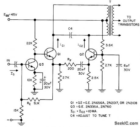
Uses modified long-tail pair to give highly stable gain. Separate emitter resistors improve bias stability. Provides push-pull operation.- Transistor Manual, Seventh Edition, General Electric Co., 1964, p 222. (View)
View full Circuit Diagram | Comments | Reading(743)
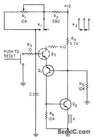
CAR_WIPER_CONTROL
Published:2009/7/3 3:42:00 Author:May
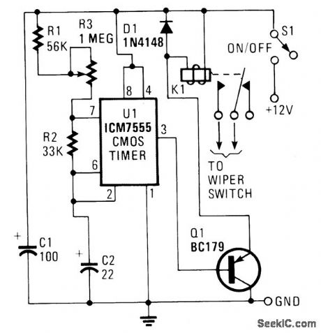
U1 is configured to operate in the standard astable mode, providing a form of relaxation oscillator. When power is applied, C2 initially charges through R1, R2 and R3 to two-thirds of the supply voltage. At that point, U1 senses that its threshold volt-age at pin 6 has been reached, and triggers the timer, causing its output at pin 3 to go high. That high, applied to the base of Q1, keeps the transistor in the off state. Now 02 begins to discharge through R2 to pin 7 of U1. When C2 has discharged to about one-third of the supply voltage, U1 is toggled back to its original state. C2 starts to charge again, as pin 3 of U1 goes low. The low at pin 3 causes Q1-which serves as an emitter-follower buffer stage-to turn on, allowing current to flow through the coil of relay K1. That, in turn, causes K1's contacts to close, applying power to the wipers. The charge time of capacitor C2 is determined by the setting of potentiometer R3. Capacitor C2 should be a tantalum type, and actually, almost any 12-volt coil relay with sufficiently heavy contacts should serve well. (View)
View full Circuit Diagram | Comments | Reading(785)
ICE_FORMATION_ALARM
Published:2009/7/3 3:31:00 Author:May
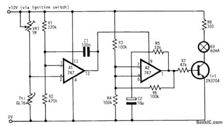
The circuit warns car drivers when the air temperature close to the ground approaches 0℃, thereby indicating possible formation of ice on the road surface. Op amp A1 is wired as a voltage level sensor. Op amp A2 is wired as an astable multivibrator which, by means of current buffer Tr1, flashes a filament lamp at about 1 Hz. As air temperature falls, a point is reached when the voltage at pin 2 just rises above the volt-age at pin 1. The output of A1 is immediately driven into positive saturation, since it is operated open loop. This positive output voltage powers A2 through its V + connection on pin 9, starting the oscillator. The thermistor is a glass bead type with a resistance of about 20 MΩ at 20℃. VR1 is adjusted so that the lamp starts flashing when the air temperature is 1 to 2℃. (View)
View full Circuit Diagram | Comments | Reading(1637)
ROAD_ICE_ALARM
Published:2009/7/3 3:27:00 Author:May
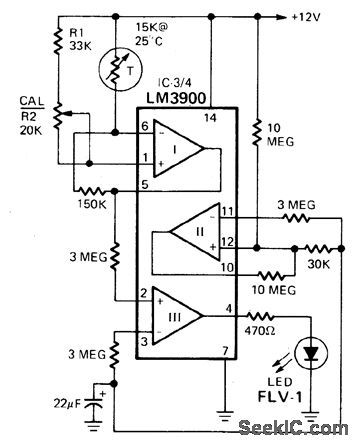
The circuit uses a thermistor and three sections of a LM3900 quad op amp IC. When the temperature drops to 36°F the LED indicator flashes about once each second. The flashing rate increases as temperature drops to 32°F when the LED remains on. Amplifier I compares the thermistor's resistance to the resistance of the standard network connected to its noninverting input. Its output-fed to the noninverting input of op amp III-varies with temperature. Op amp II is a free-running multivibrator feeding a pulse signal of about 1 Hz to the inverting input of op amp III. This amplifier compares the outputs of op amps I and II and turns on the LED when the multi-vibrator's output level drops below op amp I. The monitor is calibrated by placing the thermistor in a mixture of crushed ice and water and adjusting the 20 kΩ pot so the LED stays on. (View)
View full Circuit Diagram | Comments | Reading(1121)
POWER_SUPPLY_PROTECTION_CIRCUIT
Published:2009/7/3 3:21:00 Author:May
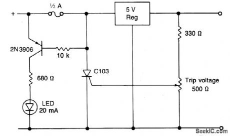
Circuit NotesWhen using a regulated supply to reduce a supply voltage there is always the danger of component failure in the supply and consequent damage to the equipment. A fuse will protect when excess current is drawn, but might be too slow to cope with overvoltage conditions. The values shown are for a 12 V supply being dropped to 5 V. The trip voltage is set to 5.7 V to protect the equipment in the event of a regulator fault. The 330 ohm resistor and the 500 ohm potentiometer form a potential divider which samples the output voltage as set by adjustment of the potentiometer. The SCR is selected to carry at least twice the fuse rating. The full supply voltage is connected to the input of the regulator. The 2N2906 is held bias off by the 10 k resistor and the SCR so that the LED is held off. If the output voltage rises above a set trip value then the SCR will conduct, the fuse will blow, and the 2N3906 will be supplied with base current via the 10 k resistor, and the LED will light up. (View)
View full Circuit Diagram | Comments | Reading(1018)
REVERSING_MOTOR_DRIVE_DC_CONTROL_SIGNAL
Published:2009/7/3 3:20:00 Author:May
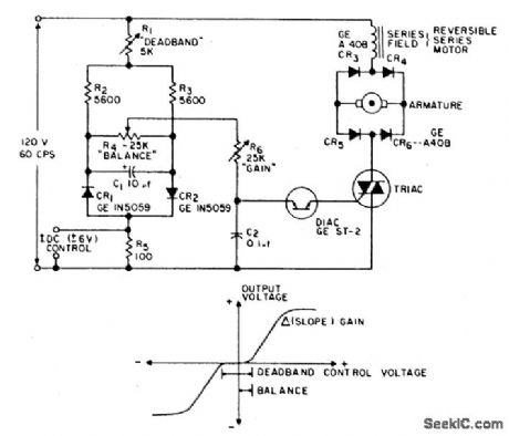
This is a positioning servo drive featuring adjustment of balance, gain, and deadband.In addition to control from a dc signal, mechanical input can be fed into the balance control, or that control could be replaced by a pair of resistance transducers for control by light or by temperature. (View)
View full Circuit Diagram | Comments | Reading(749)
| Pages:144/312 At 20141142143144145146147148149150151152153154155156157158159160Under 20 |
Circuit Categories
power supply circuit
Amplifier Circuit
Basic Circuit
LED and Light Circuit
Sensor Circuit
Signal Processing
Electrical Equipment Circuit
Control Circuit
Remote Control Circuit
A/D-D/A Converter Circuit
Audio Circuit
Measuring and Test Circuit
Communication Circuit
Computer-Related Circuit
555 Circuit
Automotive Circuit
Repairing Circuit