
Control Circuit
Index 154
DOOR_OPEN_ALARM
Published:2009/7/1 0:47:00 Author:May
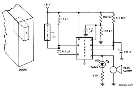
Door open alarms are used chiefly in automotive, industrial, and appliance applications. This type of circuit can sense the opening of a refrigerator door. When the door opens, a triac could be activated to control the inside light. The figure shows a door position alarm. When the door is opened, an LED turns on and the piezo alarm sounds for approximately 5 seconds. This circuit uses a TL3019 Hall-effect device for the door sensor. This normally open switch is located in the door frame. The magnet is mounted in the door. When the door is in the closed position, the TL3019 output goes to logic low, and remains low until the door is opened. This design consists of a TLC555 monostable timer circuit. The 1 μF capacitor and 5.1 M ohm resistor on pins 6 and 7 set the monostable RC time constant. These values allow the LED and piezo alarm to remain on about 5 seconds when triggered. One unusual aspect of this circuit is the method of triggering. Usually a 555 timer circuit is triggered by taking the trigger, pin 2, low which produces a high at the output, pin 3. In this configuration with the door in the closed position, the TL3019 output is held low. The trigger, pin 2, is connected to IA the supply voltage Vgg. When the door opens, a positive high pulse is applied to control pin 5 through a 0.1 μF capacitor and also to reset pin 4. This starts the timing cycle. Both the piezo alarm and the LED visual indicator are activated. (View)
View full Circuit Diagram | Comments | Reading(2920)
Floating_current_loop_transmitter
Published:2009/7/24 7:38:00 Author:Jessie
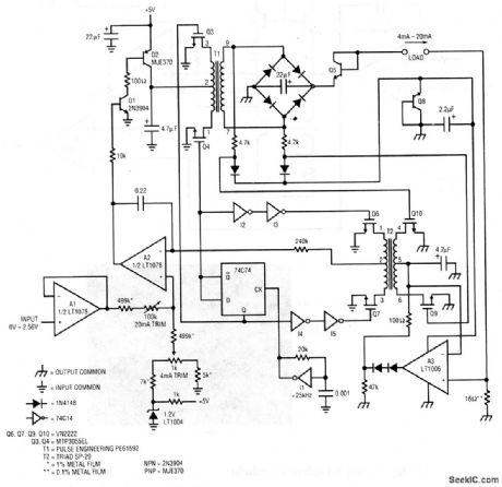
A 4- to 20-mA current-loop transmitter is frequently required in industrial process control. Because of uncertain or dangerous common-mode voltages, it is desirable that the generated current be completely galvanically isolated from the transmitter input. This circuit does this while operating from a single 5-V supply. To calibrate this circuit, apply 0-V input and adjust the 4-mA trim for 4.00-mA output (0.064 V across the 16-Ω shunt). Next, apply 2.56-V input and set the 20-mA trim for 20.00-mA output (0.3200 V across the 16-Ω shunt). Repeat this procedure until both points are fixed. Notice that the 2.56-V input range is directly compatible with D/A converter (chapter 6) outputs, which permits digital control. Linear Technology Corporation, 1991, AN45-6. (View)
View full Circuit Diagram | Comments | Reading(893)
PHOTOELECTRIC_SWITCH
Published:2009/6/30 23:51:00 Author:May
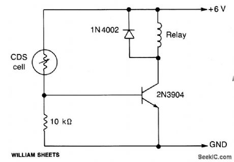
The CDS cell resistance decreases in the presence of light, turning on the 2N3904 relay driver. (View)
View full Circuit Diagram | Comments | Reading(3548)
LIGHT_OPERATED_SWITCH
Published:2009/6/30 23:50:00 Author:May
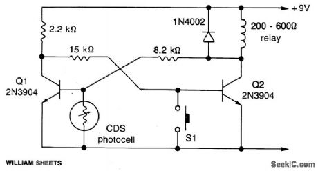
This circuit uses a flip-flop arrangement of Q1 and Q2. Normally Q1 is conducting heavily. Light on CDS photocell causes Q1 bias to decrease, cutting it off, tuming on Q2, removing the remaining bias from Q1. Reset is accomplished by depressing S1. (View)
View full Circuit Diagram | Comments | Reading(807)
PHOTO_ALARM
Published:2009/6/30 23:47:00 Author:May
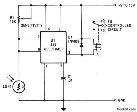
LDR1, a cadmium sulphide (CDS) photoresistive cell is used as the lower leg of a voltage divider between VCC and ground. The timer terminals 2 and 6 are connected to the junction of the photocell and SENSITIVITY control R1. The resistance of the photoresistive cell varies inversely as the light intensity; resistance is high when the illumination level' is low; low in bright light. (The Radio Shack CDS cell 276-116 has a typically wide resistance range-about 3 megohms in darkness and 100 ohms in bright light.) When the light is interrupted or falls below a level set by SENSITIVITY control R1, the rise in LDRl's resistance causes the voltage on pins 2 and 6 to rise. If the control is set so the voltage rises above 2/3 VCC, the relay pulls in. The relay drops out when the light level increases and the drop across the photocell falls below 2/3 VCC. (The circuit can be modified by placing relay K1 and diode Dl between pin 3 and ground. In this case, the relay drops out when the voltage on pins 2 and 6 rises above 2A Vgg, and pulls in when it falls below 1/3 VCC . This modification is valuable when the relay has single-throw contacts.) Opening and closing of the relay contacts occurs at different illumination levels. This 1/3 VCC hysteresis is an advantage that prevents the circuit from hunting and the relay from chattering when there are very small changes in illumination. (View)
View full Circuit Diagram | Comments | Reading(1122)
ALARM_FOR_DIGITAL_CLOCK
Published:2009/6/30 23:16:00 Author:May
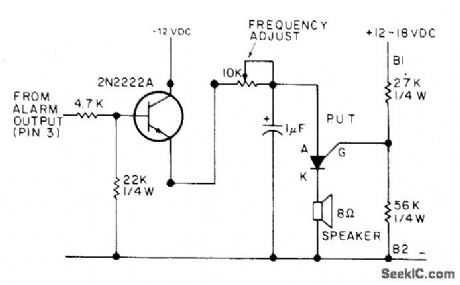
Uses transistor as driver to turn on programmable unijunction transistor (PUT) oscillator feeding 8-ohm loud-speaker. Pitch of tone can be adjusted with 10 K pot. Input is from alarm pin of digital clock IC (pin 3 for Fairchild FCM7001 equivalent of Cal-Tex CTT001}. PUT is Radio Shack 276-119 or equivalent.-W. J. Prudhomme, CT7001 Clock-buster, 73 Magazine, Dec. 1976, p 52-54 and 56-58. (View)
View full Circuit Diagram | Comments | Reading(2828)
2_kW_FLASHER_WITH_PHOTOELECTRIC_CONTROL
Published:2009/6/30 23:13:00 Author:May
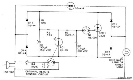
CR1, CR2, CR3, and CR4 form a bridge circuit with the SCR across the dc legs.With light on the photoconductor PC1, C1 charges through R1 to about 150 Vdc. The resistance of PC1 is low when illuminated, so very little voltage appears across it or C2. At about 90 volts C1 starts discharging through RI and the SCR, but the SCR cannot turn off until C1 is almost completely discharged. When the SCR turns off during the interval line voltage is near zero, the full supply voltage again appears across the bridge, and C1 charges again to a high voltage. The voltage on C2 also starts rising until the neon lamp fires and the cycle repeats. An alternative remote control can be made by adding a second neon lamp, N2, and masking the photocell so it sees only N2. A very sensitive remote control is thus obtained that is completely isolated from the load circuit.For low-voltage remote control a flashlight lamp may be used instead of N2 and operated at about 1/2 its normal voltage thus giv.ing exceptionally long life. Performance of the photoelectric control may be inverted (flash when the photoconductor is illuminated) by interchanging PC1,and R2.Sensitivity in either the normal or inverted modes can be decreased by partially masking PC1, and can be increased by increasing resistor R2 to about 470 K. To increase on time, increase C1; to increase off time, increase R3. (View)
View full Circuit Diagram | Comments | Reading(657)
6-DIGIT_WITH_CALENDAR_AND_ALARMS
Published:2009/6/30 22:55:00 Author:May

Circult is built around Cal-Tex CT7001 IC that includes outputs for displaying day of monthalong with time on Liftonix DL707 LED read-outs. Transistor switch Q1 and relay form timer triggered by IC to control radio or other appli-ance drawing up to 5 A from AC Iine. Dual-volt-age power supply provideg 7 and 14 VDC. Includes snooze alarm along with regular built-intransistor-driven buzzer.-M. s. Robbins, Electronic Clocks and Watches, Howard W.Sams, Indianapolis,IN,1975,p 103-104 and116-117. (View)
View full Circuit Diagram | Comments | Reading(1337)
MICROPROCESSOR_SELECTED_PULSE_WIDTH_CONTROL
Published:2009/6/30 22:44:00 Author:May
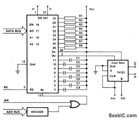
Differential multiplexers are generally used in process control applications to eliminate errors due to common mode signals. In this circuit however, advantage is taken of the dual multiplexing capability of the switch. This is achieved by using the multiplexer to select pairs of RC networks to control the pulse width of the multivibrator. This can be a particularly useful feature in process control applications where there is a requirement for a variable width sample window for different control signals. (View)
View full Circuit Diagram | Comments | Reading(665)
CONTROL_AT_LOW_GAIN_LEVELS
Published:2009/6/30 22:22:00 Author:May
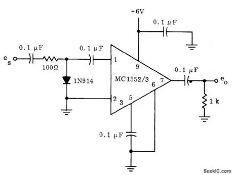
Diode is used as variable impedance in voltage-divider network at input of video amplifier to provide AGC at lower gain levels than could be handled with more conventional external-diode circuits. Voltage gain for Motorola MC1552 decreases from about 50 for 1-mA AGO control current to about 20 for 8 mA. For MC1553 high-gain video amplifier, gain drops from 400 at 1 mA to 25 at 8 mA.- A Wide Band Monolithic Video Amplifier, Motorola, Phoenix,AZ, 1973, AN-404 p 11. (View)
View full Circuit Diagram | Comments | Reading(856)
AGC_WITH_MANUAL_CONTROL
Published:2009/6/30 22:13:00 Author:May
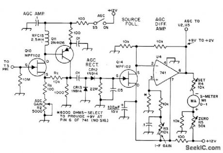
Used in 1.8-2 MHz communication receiver having wide dynamic range. R3 serves as manual IF gain control. R2 provides gain variation from 6 to 40 dB for AGO amplifier. Delay is about 1 s. Input is taken from primary of transformer that drives product detector of receiver, and AGC output goes to CA3028A IF opamp. Two-part article gives all other circuits of receiver.-D. DeMaw, His Eminence-the Receiver, QST, Part 2-July 1976, p 14-17 (Part 1-June 1976, p 27-30). (View)
View full Circuit Diagram | Comments | Reading(1026)
DC_VOLTAGE_TO_TIME
Published:2009/6/30 21:02:00 Author:May
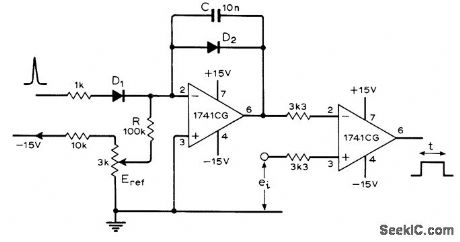
Opamp connected as integrator feeds opamp comparator to produce output pulse whose width is proportional to magnitude of DC input voltage. Circuit shown is for positive inputs only; for both positive and negative inputs, article tells how to add another comparator. Circuit can then be used to generate start and stop pulses applied to digital timer of digital voltmeter.—G. B. Clayton, Experiments with Operational Amplifiers, Wireless World, Sept. 1973, p 447-448. (View)
View full Circuit Diagram | Comments | Reading(942)
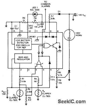
LINE_OPERATED_PHOTO_ELECTRICSMOKE_ALARM_USING_LIGHT_SENSITIVE_RESISTOR(INCLUDESDETEC_TION_OF_OPEN_CIRCUITED_LED)
Published:2009/6/30 3:51:00 Author:May
View full Circuit Diagram | Comments | Reading(793)
ELECTRONIC_COMBINATION_LOCK
Published:2009/6/30 3:17:00 Author:May
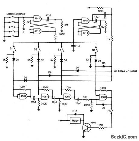
Switches S1 through S5 must be operated In rapid sequence to operate the lock,They can be any numbers on a 10-button switch pad.If an Incorrect button is pushed,alarm sounds and the circuit is disabled for two minutes. (View)
View full Circuit Diagram | Comments | Reading(1)
POWER_FAILURE_ALARM_1
Published:2009/6/30 3:16:00 Author:May
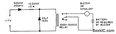
While the power is on,the relay is held open,but when the power fails the buzzercircuit contacts close. (View)
View full Circuit Diagram | Comments | Reading(727)
ULTRASONIC_SWITCH
Published:2009/6/30 3:12:00 Author:May
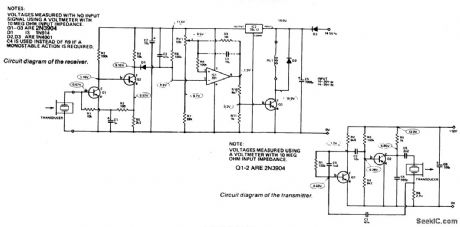
Receiver. Output from the transducer is amplified by Q1 and Q2, and rectified by D1. Voltage on pin 2 of IC1 will go more negative as the input signal increases. IC1 is used as a comparator and checks the voltage on pin 2 (i.e., the sound level), to that on pin 3 which is the reference level. If pin 2 is at a lower voltage than pin 3 (i.e., a signal is present), the output of IC1 will be high (about 10.5 volts) and this will turn on Q3 which will close the relay. The converse occurs if pin 2 is at a higher voltage than pine 3.Transmitter. The oscillator frequency is determined by the transducer characteristics [(minimum (series resonance) at 39.8 kHz fol-lowed by a maximum (parallel resonance) at 41.5 kHz.)] Two transistors from a noninvert-ing amplifier and positive feedback is supplied via the transducer, R6 and C3. At the series resOnant frequency, this feedback is strong enough to cause oscillation. (View)
View full Circuit Diagram | Comments | Reading(952)
POWER_FAILURE_ALARM
Published:2009/6/30 3:12:00 Author:May
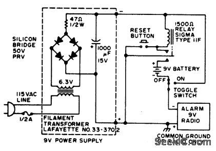
If the power fails, the radio alarm goes on. No loud siren, bell, or whistle. Even if the power is restored, the alarm stays on until RESET button is pushed. (View)
View full Circuit Diagram | Comments | Reading(208)
9_BIT_USING_DIGITAL_SWlTCHES
Published:2009/6/30 2:58:00 Author:May
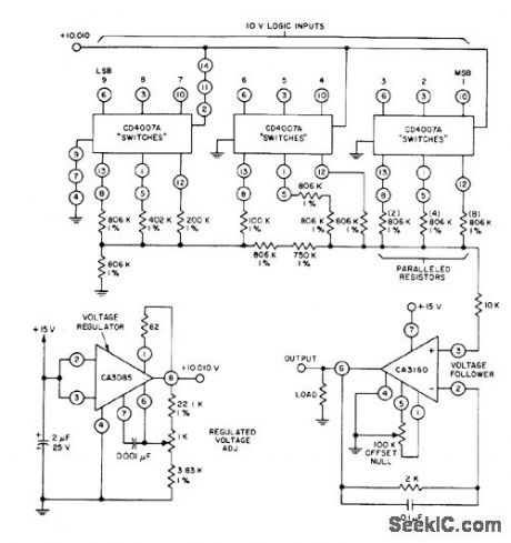
Combination of CD4007A multiple-switch CMOS ICs, ladder network of discrete metal-oxide film resistors, CA3160 voltage-follower opamp, and CA3085 voltage regulator gives digital-to-analog converter that is readily interfaced with 10-V logic levels of CMOS input. Required resistor accuracy, ranging from ±0.1% for bit 2 to ±1% for bits 6-9, is achieved by using series and parallel combinations of 806K resistors.— Linear Integrated Circuits and MOS/FET's, RCA Solid State Division, Somerville, NJ, 1977, p 267-268. (View)
View full Circuit Diagram | Comments | Reading(981)
FLASHER_LIGHT_CONTROL
Published:2009/6/30 2:55:00 Author:May
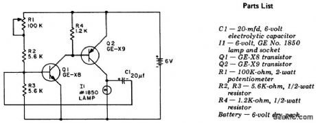
Circuit NotesThe circuit is a two-stage, direct-coupled transistor amplifier connected as a free-running multivibrator. Both the flash duration and flash interval can be changed by turning the potentiometer, R1. (View)
View full Circuit Diagram | Comments | Reading(561)
HI_FI_TONE_CONTROL_CIRCUIT_HIGH_Z_INPUT
Published:2009/6/30 2:48:00 Author:May
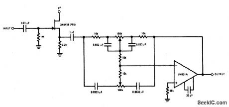
The 2N5458 JFET provides the function of a high input impedance and low noise characteristics to buffer an op amp feedback tone control circuit. (View)
View full Circuit Diagram | Comments | Reading(814)
| Pages:154/312 At 20141142143144145146147148149150151152153154155156157158159160Under 20 |
Circuit Categories
power supply circuit
Amplifier Circuit
Basic Circuit
LED and Light Circuit
Sensor Circuit
Signal Processing
Electrical Equipment Circuit
Control Circuit
Remote Control Circuit
A/D-D/A Converter Circuit
Audio Circuit
Measuring and Test Circuit
Communication Circuit
Computer-Related Circuit
555 Circuit
Automotive Circuit
Repairing Circuit