
LED and Light Circuit
Index 39
PREHEATING_PROGRAMMED_LAMPS
Published:2009/7/12 23:54:00 Author:May
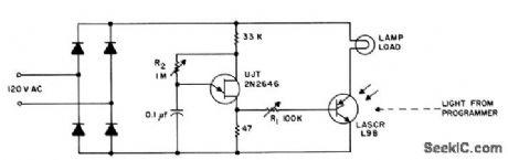
Minimizes thermal stresses on lamps and controls when programmed operation is repetitive for large number of cycles. Ujt control circuit provides preheating of lamp by triggering light-activated scr late in each half cycle. Setting of R2 determines minimum lamp current to maintain filament temperature just below visible leveL- Silicon Controlled Rectifier Manual, Third Edition, General Electric Co.1964, p216. (View)
View full Circuit Diagram | Comments | Reading(860)
LONG_INTERVALS_WITH_SMALLC
Published:2009/7/12 23:35:00 Author:May
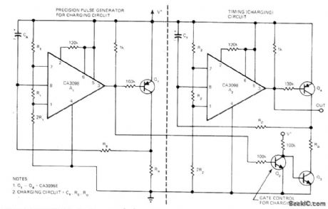
Use oftwo CA3098 dual-input precision level detectorseliminates need for expensive high-capacitance low-leakage timing capacitors when delay intervals of several hours are required. For 4-h timer, CT is only 16 μF if Rc is 22 megohms and RD is 100 kilohms. Article traces circuit operation and gives design equations.-G. J. Granierl,Precision Level Detector IC Simplifies control Circuit Design,EDN Magazine, Oct 5,1975,p 69-72. (View)
View full Circuit Diagram | Comments | Reading(1228)
DUAL_LAMP_DRIVER
Published:2009/7/12 21:59:00 Author:May
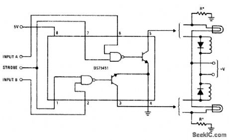
National DS75451 dual peripheral AND driver using positive logic provides up to 300 mA per section for driving incandescent lamps. Optional keep-alive resistors R maintain OFF-state lamp current at about 10% of rated value to reduce surge current.Lamp voltage depends on lamps used. Relays shown, with diodes across solenoids, can be used in place of lamps if desired.- Interface Databook, National Semiconductor, Santa Clara, CA, 1978, p 3-20-3-30. (View)
View full Circuit Diagram | Comments | Reading(798)
INEXPENSIVE_EMERGENCY_LIGHT
Published:2009/7/17 1:41:00 Author:Jessie

This low-cost circuit charges two nickel-cadmium cells to provide a standby power supply for a two-lamp emergency light, which is automatically switched on in the event of a power failure. Diode D1 and smoothing capacitor C1 form a conventional single-phase rectifier circuit with an output voltage of about 6 V. This voltage is used to continuously charge two series-connected NiCd batteries with a current of 80 to 100 mA, which flows via R1 and D2. At this rate, a 2-Ah (ampere-hour) NiCd battery can be safely charged for extensive periods. The voltage drop across D2 reverse-biases the base-emitter junction of PNP transistor T1. Consequently, the transistor is turned off, and the lamps connected, to its collector do not light. When a power outage occurs, T1 is supplied with base current (from the batteries) via R2, whereupon the miniature lamps are turndd on. As soon as the power is restored, T1 is switched off again, and the batteries are charged again via RI and D2. (View)
View full Circuit Diagram | Comments | Reading(3327)
ISOLATED_RS232_INTERFACE
Published:2009/7/12 21:00:00 Author:May
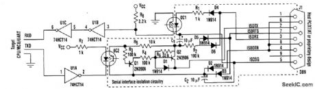
Electrical isolation of 1500 V or higher is possible with this cost-effective RS232 interface. It is ideal for various data-communication designs, including medical instrumentation and devices within harsh electrical environments. The interface uses the host's TXD (transmit data), RXD (receive data), DTR (data terminal ready), and RTS (request to send) lines to provide power.For fully duplexed operation, the host's communications port should be set up so that its RTS is off (at negative voltage). Halfduplex operation can use the host's TXD negative voltage, available through D6, to run the circuitry. Sending a low bit (space state) to the host is just the opposite. This time, the required positive voltage is supplied from the host via diodes D2 and D3, and is routed through Q1 and D1 to DB9-2. (View)
View full Circuit Diagram | Comments | Reading(1712)
LED_DISPLAY_FOR_ASCLL_CODE
Published:2009/7/11 3:07:00 Author:May
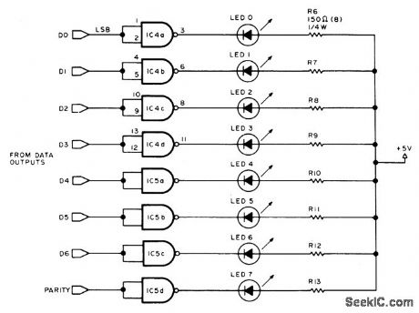
Shows code for any ASCLL keyboard character as aid in debugging keyboard matrix wiring. Requires only two 7400 quad NAND gates, eight resistors, and eight LEDs. High input to gate forces output low, grounding LED and lighting it. On standby with positive logic, all LEDs are lit with negative logic ,all are dark on stangby .arrange LEDs on keyboard so rightmost LED represents least significantbit (DO)and leftmost LED represents parity bit. Using positive logic, ASCLL code for any depressed key will show as lit LED for 1 and dark LED for o. Pin 14 of 7400 is +5 V, and pin 7 is ground.-B. Brehm. Using a Keyboald ROM, BYTE, May 1977, p 76-.82. (View)
View full Circuit Diagram | Comments | Reading(1561)
MODEL_RAILWAY_CROSSING_LIGHTS
Published:2009/7/17 3:34:00 Author:Jessie
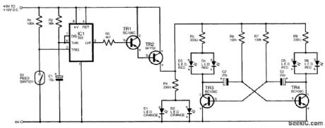
The circuit is for use on model railway layouts and approximates the flashing light signals used at level crossings. It is operated by a reed switch (S1) embedded in the track, which is closed by a magnet on the underside of a passing train. This triggers the monostable timer IC1, which powers a Darlington transistor pair (TR1 and TR2). Diodes D1 and D2 (orange) illuminate, and also TR3 and TR4, connected as an astable, cause the red LEDs D3 to D6 to flash alternately for about 6 s, long enough for the train to pass. One set of LEDs is used on each side of the level crossing, for added realism. For 00 scale, 3-mm LEDs are best. (View)
View full Circuit Diagram | Comments | Reading(3020)
MODEL_SPORTS_CAR_LIGHTING_SYSTEM
Published:2009/7/17 3:30:00 Author:Jessie
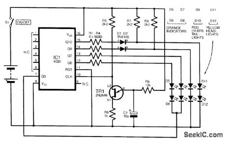
In order to add some realism to a model sports car, this simple circuit can be built into virtually any type of toy car, battery-operated or not. The design uses a CD4020 14-stage binary counter to operate LED tum indicators (D5 to D8), taillights (D9 and D10), and headlights (D11 and D12). The counter IC1 is clocked by a unijunction oscillator based around TR1. The red taillights and the yellow headlights draw a small current, supplied constantly by resistors R7 and R8. For added re-alism, this current is supplemented through resistors R1 and R2 to give an impression of headlights dipping and taillights braking. The model's turn indicators flash whenever they are enabled, and so the cathodes (k) of D5 to D8 are taken to another output (Q3, pin 7) of IC1. With their anodes (a) taken positive via resistors R3/R4 and the relevant counter output, they flash at the rate determined by Q3. The result is that one set of indicator lights flashes, then the other set, followed by both. The circuit is powered by a PP3-type or MN1604 9-V battery, and a small slide switch S1 can be mounted on the vehicle's underside. (View)
View full Circuit Diagram | Comments | Reading(5148)
UJT_BISTABLE_WITH_CLAMP
Published:2009/7/17 4:05:00 Author:Jessie
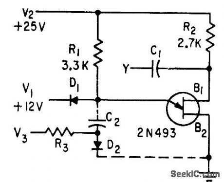
Clamping diode holds emitter voltage below peak-point voltage. When negative trigger at base B2 turns on transistor, D2 is back-biased and R1 becomes emitter load. Operation is stable if capacitance between emitter and base B1 is kept below critical value.-T. P. Sylvan, Bistable Circuits Using Unijunction Transistors, Electronics, 31:51, p 89-91. (View)
View full Circuit Diagram | Comments | Reading(918)
SIMPLE_TEMPERATURE_INDICATOR
Published:2009/7/11 0:29:00 Author:May

For the absolute measurement of temperatures, a thermometer is indispensable. However, in many situations, an absolute value is not needed and a relative indication is sufficient. It would be a further advantage if a green light would indicate that all is well as far as temperature is concerned. As the tempera-ture rises, the light should change color slowly to indicate that the equipment is getting too hot.This circuit does this and works directly from the mains. The indicator proper is a two-color LED (Dl), while the sensor is a combination of a negative-temperature coefficient (NTC) and a positive-tem-perature coefficient (PTC) resistor (R4 and R3, respectively).At a relatively low temperature, the value of R3 is low and that of R4 is high. During the positive half cycle of the mains voltage, a voltage will exist across R3/D2 that is sufficiently high to cause the green section of D1 to light. The value of R3 has been chosen to ensure that during the negative half cycle of the mains voltage, the potential across it is too low to cause the red section of D1 to light.If the temperature rises, the value of R4 diminishes and that of R3 rises. Slowly, but surely, the green section will light with lesser and lesser brightness. At the same time, the red section lights with greater and greater brightness until ultimately only the red section will light.Resistor R2 and capacitor C1 ensure that the current drawn by the LEDs does not become too large. This arrangement keeps the dissipation relatively low. Both R3 and R4 should be of reasonable dimen-sions-approximately 6 mm in diameter, not less. At 25℃, the NTC must be 22 to 25 kΩ and the PTC must be 25 to 33 0. The circuit should be treated with great care because it carries the full mains voltage. (View)
View full Circuit Diagram | Comments | Reading(1183)
GRAND_PRIX_STARTING_LIGHTS_
Published:2009/7/17 3:46:00 Author:Jessie
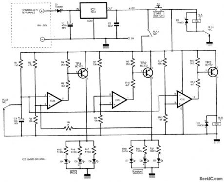
The figure shows a circuit design for a starting gantry with three red and three green starting lights. It can be powered from the racing set's power-supply unit. A 12-V regulator (IC1) provides a stabilized supply for the circuit and diode D1 prevents accidental reverse connection by the young motor enthusiast. The circuit uses a system of relays to start and stop the sequence. When START switch S1 is pressed, relay contacts RLA1 close and this applies +12 V to the sequencer and also latches the relay. Contacts RLA2, across capacitor C3, open. Three comparators are used (IC2a, IC2b, and IC2c), and their noninverting (+) terminals each have a reference voltage set by a potential divider at about +2.10 V, +2.75 V, and +4.75 V, respectively. Either an LM339 quad comparator or an LM324 quad op amp can be used. When capacitor C3 charges in excess of +1.75 V, transistor TR1 conducts and the red LEDs D4 to D6 illuminate. At +2.75 V, TR2 conducts and the green LEDs D7 to D9 light. IC2a also swings high, via resistor R6, and so the red lamps extinguish. When capaci-tor Ct reaches +4.75 V, transistor TR3 conducts and completes the circuit to relay RLB. Contacts RLB1 (normally closed) now open and disconnect relay RLA. Contacts RLA2 then close, which dis-charges the timing capacitor C1, ready for next time. (View)
View full Circuit Diagram | Comments | Reading(1164)
MODEL_RAILROAD_LIGHTHOUSE_LAMP_SIMULATOR
Published:2009/7/17 3:39:00 Author:Jessie
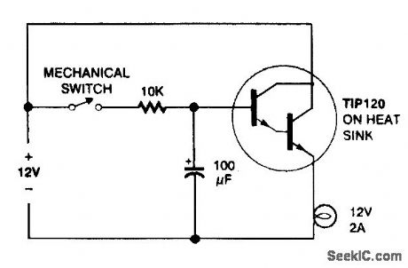
The lamp turns on and off gradually, controlled by the charging and discharging of the capacitor. Here is a circuit that will do the job. It uses a TIP120 power transistor as a voltage-regulating element. The voltage across the lamp is always 1.2V lower than the voltage across the capacitor. Closing the switch charges the capacitor gradually over a period of a few seconds, causing the voltage to go up. When the switch opens, the capacitor slowly discharges and the voltage goes down again. You might have to experiment with component values to get the effect you want. The capacitor controls both the rise time and the fall time; the resistor controls the rise time only. In both cases, larger values make the action go more slowly. Be sure to mount the TIP120 transistor on a heatsink, and remember that its mounting hole is connected to the collector (and thus to +12 V in the circuit). (View)
View full Circuit Diagram | Comments | Reading(2623)
MULTITRACE_CRO_DISPLAY
Published:2009/7/10 23:06:00 Author:May
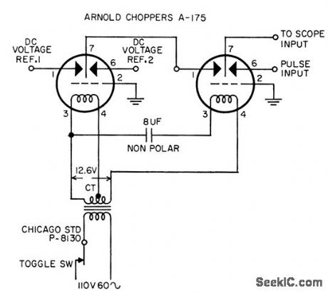
Allows simullaneous presentaion of desired pulse and of limit voltage levels Choppers operate 45°out of phase, which Provides approximately equal brightness for both parts of display.-D F.Frost and R. M. Zilberstein, Multitrace Display Device, EEE, 10:8, p27. (View)
View full Circuit Diagram | Comments | Reading(761)
PHONE_MESSAGE_FLASHER
Published:2009/7/10 22:26:00 Author:May
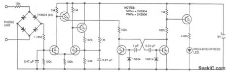
This circuit flashes an LED to indicate that your phone rang during your absence. A differential amplifier with hysteresis (Q1, Q2, and Q3) detects high line voltage(ringing), which turns on Q4, mulitvibrator Q5/Q6, and flashes the LED via Q7. Q1 and Q2 remain on until the phone-line voltage drops to less than 9 V, which indicates an off-hook condition. (View)
View full Circuit Diagram | Comments | Reading(1041)
B_H_LOOP_DISPLAY
Published:2009/7/10 22:21:00 Author:May
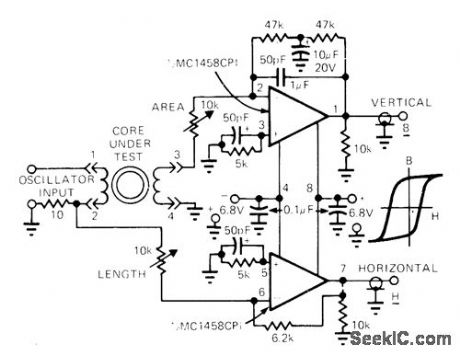
Low-cost dual opamp circuit allows display of hysteresis loop on call-brated XY oscilloscope. Two windings are placed on core to be tested, with opamp of fluxmeasuring system connected to secondary for deriving vertical deflection input representing flux B. Artide gives design equations and details of circuit operation and use.-D. A. Zinder, X-Y Oscilloscope Displays Hysteresis Loop of Any Core, EDN Magazine, Feb. 5, 1975, p 54-55. (View)
View full Circuit Diagram | Comments | Reading(1508)
EMITTER_FOLLOWER_LED_DRIVER
Published:2009/7/10 5:30:00 Author:May
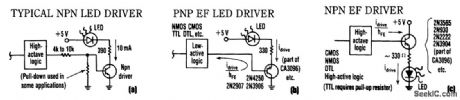
Using emitter/followers saves parts and simpliftes LED driver loading on logic circuitry. (View)
View full Circuit Diagram | Comments | Reading(1004)
RF_OUTPUT_INDICATOR
Published:2009/7/10 5:28:00 Author:May

A simple RF detector circuit using a visual indicator can be useful for an RF output indicator, etc.This circuit was used for a transmitter ON indicator. (View)
View full Circuit Diagram | Comments | Reading(0)
MICROPOWER_ONE_WAY_INTERCOM_
Published:2009/7/10 4:47:00 Author:May
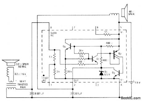
National LM3909 IC operating from single 1.5-V cell serves as low-power one-way intercom suitable for listening-in on child's room and meeting other room-to-room communication needs. Battery drain is only about 15 mA. Person speaking directly into 3.2-ohm loudspeaker used as microphone delivers full 1.4 V P-P signal to 40-ohm loudspeaker at listening location.- Linear Applications, Vol. 2, National Semiconductor, Santa Clara, CA, 1976, AN-154, p 9. (View)
View full Circuit Diagram | Comments | Reading(1104)
PRECISION_INTEGRATOR
Published:2009/7/10 4:16:00 Author:May
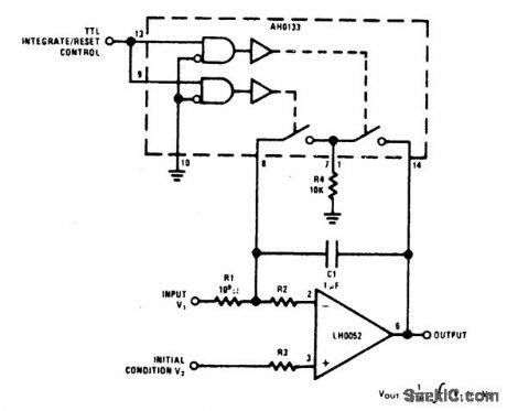
Low input bias current of Natiortal LH0052 opamp makes it suitable for applioations requiring long time con stants. R1 is selected so total leakage current at summing mode is sufficiently smaller than sig-nal current to ensure required accuracy. R2 is included to protect input circuit during reset ransient but can be omitted for low-speed applications. R3, used to balance resistance in inputs, should be equal to sum of R2 and 100-ohm resistance of reset switch.- Linear Applications, Vol. 1, National Semiconductor, Santa Clara, CA, 1973, AN-63, p 1-12.
(View)
View full Circuit Diagram | Comments | Reading(891)
as_CURRENT_INDICATOR
Published:2009/7/10 3:58:00 Author:May
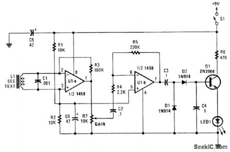
Using a dual op amp driving a rectifier and emitter-follower, this circuit indicates ac current on an LED. L1 is an audio transformer winding using a pick-up coil, or 100 to 200 turns of #28 gauge wire 2 in diameter, etc. The circuit can trace ac lines behind walls, etc. or detect ac current flow. (View)
View full Circuit Diagram | Comments | Reading(4608)
| Pages:39/72 At 202122232425262728293031323334353637383940Under 20 |
Circuit Categories
power supply circuit
Amplifier Circuit
Basic Circuit
LED and Light Circuit
Sensor Circuit
Signal Processing
Electrical Equipment Circuit
Control Circuit
Remote Control Circuit
A/D-D/A Converter Circuit
Audio Circuit
Measuring and Test Circuit
Communication Circuit
Computer-Related Circuit
555 Circuit
Automotive Circuit
Repairing Circuit