
Measuring and Test Circuit
Index 38
ELECTROSCOPE_CIRCUIT
Published:2009/7/16 4:46:00 Author:Jessie


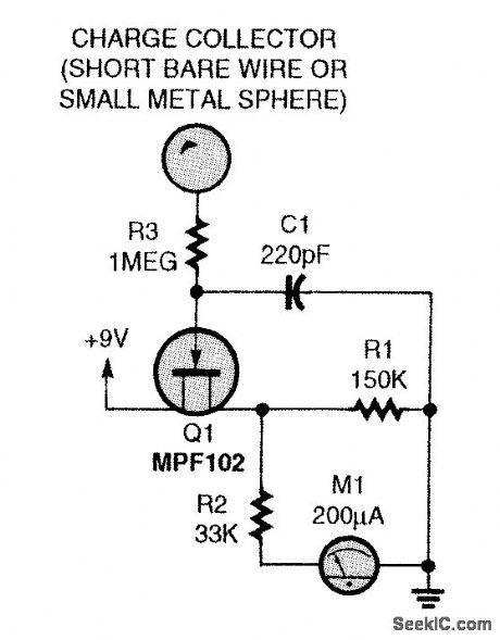
This circuit detects a charged object at a respectable distance and displays the polarity (positive, negative, or earth-grounded) and relative intensity. In operation, C1 reduces ac noise but lowers the sensitivity a bit. The MPF102 and R1 form a voltage divider. When the FET's gate is earth-grounded, the divider's output will be about 4.5V, giving a half-scale reading on M1, a 200-μA meter. A positively charged object (like cotton-rubbed glass) will give a positive deflection from half scale, and a negatively charged object (a plastic comb, for example) will give a negative meter deflection. The whole circuit (including the 9-V supply) should be in a metal enclosure. (View)
View full Circuit Diagram | Comments | Reading(1252)
CURRENT_LIMITERS
Published:2009/7/13 2:23:00 Author:May

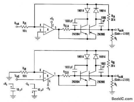
A user-controlled internal current limit on power op amps isn't always provided by manufacturers. However, the current limit can be set extemally by using the technique shown, in which the output current is sensed with a single resistor. The resistor activates a complementary transistor switch that reduces irtverting gain, lirrtiting output current. The technique is demonstrated with 8-pin OPA2541 or OPA2544 dual-power op amps that are lacking an intemal user-controlled current limit. The extemal components add an adjustable current limit to these amplifiers. The PNP transistor controls the positive current limit, and the NPN transistor controls the negative current limit. Both transistors are 0FF until the voltage drop across RCT reaches the current-limit set point. At the current-limit set point, current from the controlling transistor will sum with the input current (through Ri) at the op amp's inverting input summing junction. This will limit the output. The diodes in series with the collectors of both transistors prevent forward base-collector bias. High-frequency oscillation during current limit is damped out with the 1000-pF capacitors. These capacitors only nominally affect the conftguration's closed-loop bandwidth because the diodes, which are normally off, isolate them. (View)
View full Circuit Diagram | Comments | Reading(1266)
5_V_TO_12_V_1_A_DC_TO_DC_CONVERTER
Published:2009/7/13 2:19:00 Author:May
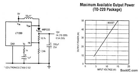
Local on-board conversion from 5 V to 12 V for use in amplifier, signal conditioning, or bus driver circuitry normally entails the use of a module or complex dc-to-dc converter design. The LT1269 100-kHz PWM switching regulator can provide a minimum of 1 A at a regulated 12 V in a surface-rnountable DD package (500 mA in 20-lead, small-outline SMT). Included on the chip is a low-ON-resistance switch (0.33 Ω) with a 4-A current limit for high-efficiency conversion in the boost converter shown here. The high switching frequency permits the use of small inductors and capacitors in this converter. The device can be placed in a micropower shutdown mode (100 μA typical supply current) by activating a clamp on the VC pin. (View)
View full Circuit Diagram | Comments | Reading(926)
OP_AMP_ERROR_CURRENT_MEASUREMENT_CIRCUIT
Published:2009/7/13 2:07:00 Author:May
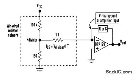
Using an air-wired resistor-divider network, designers can make a precision femtoampere source that can inject a known error current into the amplifier to check the circuit's accuracy. (View)
View full Circuit Diagram | Comments | Reading(1015)
FET_TESTER
Published:2009/7/16 20:49:00 Author:Jessie
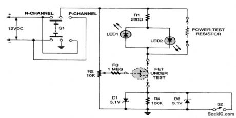
In operation, either a P-channel or an N-channel FET can be plugged in and tested by selecting the proper polarity with the power switch. With the control potentiometer (R2) at ground potential, the FET under test will conduct until the pinchoff voltage is reached. The LED will not turn on at this point because of the low current. This pinchoff voltage can be read at the top of resistor R4 with a high-impedance voltmeter. Increasing the potentiometer will decrease the pinchoff voltage until the FET conducts and an LED turns on. The LEDs give a rough indication of conduction. A more accurate reading is obtained by monitoring the voltage drop across the drain resistor. For a quick go/no-go FET check, the switch (S2) across the zeners can be closed. The associated LED should light and should go out when the switch is opened. If it does not, the FET is bad or is connected wrong, or the selector switch is set for the wrong-polarity FET. The 1-MΩ resistor (R3) at the gate connection is protection for the potentiometer should a unit under test short, it provides current limiting for the protection diodes in the gate of the CMOS FETs. (View)
View full Circuit Diagram | Comments | Reading(0)
SIMPLE_TRANSISTOR_CHECKER
Published:2009/7/16 20:47:00 Author:Jessie
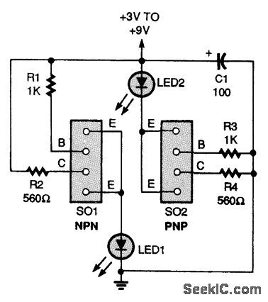
When a T092-type transistor is placed in the correct socket, if the transistor is good, the circuit turns on, according to the kind of transistor being tested. For example, if a good NPN unit is tested, LED1 turns on. Note that two emitter positions are in each socket. Transistors have different pin configurations. Some are BBC, and some are ECB. If you don't know the configuration, you can test all the possible pin positions until an LED turns on. You'll need to know if the transistor is an NPN or a PNP type, however. The supply voltage can be 3 to 9 V. There is no power switch because, without a socketed transistor, capacitor C1 is the only load on the battery. For the sockets, use an eight-pin, mini-DIP socket. (View)
View full Circuit Diagram | Comments | Reading(1506)
LED_TEST_CIRCUIT
Published:2009/7/16 20:45:00 Author:Jessie


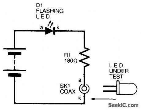
The circuit is intended as a simple one to enable spot testing of bulk surplus LEDs. A flashing LED is used (D1) with a 9-V battery, and is connected to a coaxial socket. When a test LED is placed across the socket (anode to the inner conductor), both the flashing LED and the test LED will flash. No on-off switch is necessary (View)
View full Circuit Diagram | Comments | Reading(1411)
FILM_BREAK_DETECTOR
Published:2009/7/13 1:37:00 Author:May

Photographic film in processor is run through resonant acoustic chamber in which presence of film affects en energy transfer between crystal transducers.Change in transducer output when film breaks is used to operate relay through amplifier and detector, to control automatic film processor and thereby minimize rethreading and film spoilage. Can also be used to detect bubbles in rubber tubing during blood transfusions, and detect similar changes in other films, liquids, and gases.-E. L. WIthey and R. G. Seed, Acoustic Cavity Detects Breaks in Film, Electronics,31:13,p50-51. (View)
View full Circuit Diagram | Comments | Reading(974)
DIODE_MATCHING_CIRCUIT_I
Published:2009/7/16 20:41:00 Author:Jessie
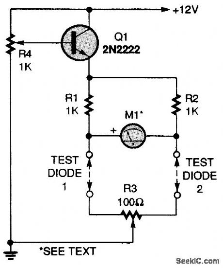
A 2N2222 transistor is connected in an emitter-follower circuit that is powered by a 12-Vdc source. Potentiometer R4 sets the voltage feeding the diodes under test. Two 1000-0,1percent resistors, RI and R2, make up two legs of a four-element bridge circuit. The diodes you want to test make up the other two legs. Potentiometer R3 is a fine-balance control. Meter M1is a 100-0-100-μA, center-zero unit. Connect jumpers in place of the test diodes, set RC to midposition, and set R4 to its maximum-voltage position (minimum resistance).Apply power and adjust R3 for a zero meter reading. Disconnect the power, set R4 to its minimum-voltage position (maximum resistance), and connect two diodes in the test positions. Slowly in-crease the bridge voltage with R4 and watch the meter for any change. The diodes are perfectly matched if the meter remains at zero as the voltage is increased. (View)
View full Circuit Diagram | Comments | Reading(1593)
SIMPLE_WATTMETER
Published:2009/7/16 20:37:00 Author:Jessie
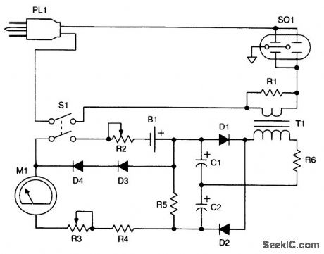
A current transformer (T1) is used to derive a larger ac voltage, which is rectified by D1and D2 to produce a dc voltage proportional to ac line current. B1, R2, and D3, and D4 are used to linearize the circuit. (View)
View full Circuit Diagram | Comments | Reading(990)
AC_WATTMETER_CIRCUIT
Published:2009/7/16 20:35:00 Author:Jessie
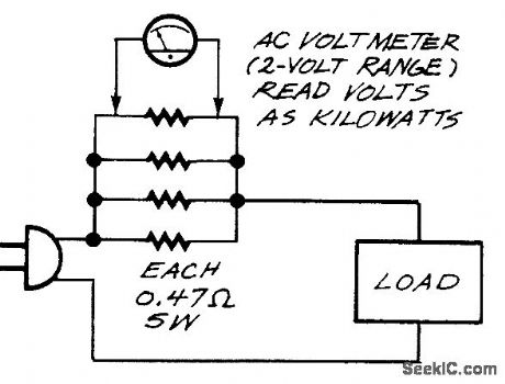
A true wattmeter is a complicated instrument. But if all the wattages that you want to measure are at the same voltage (120 Vac) and the loads are resistive (such as lights, heaters, or motors under load), you can just pass the current through at 0.12-Ω resistance (four 0.47-Ω, 5-W resistors in parallel), connect an ac voltmeter across the resistance, and read volts as kilowatts. That is, every volt across the resistance corresponds to 1000 W (equal to 8 A) drawn by the load. Remember that the voltmeter terminals are hot; use insulated pin sockets so that you won't touch the contacts accidentally. On inductive or capacitive loads, such as unloaded motors or transformers and computer power supplies, your wattmeter will read high because the current and voltage are not in phase. (View)
View full Circuit Diagram | Comments | Reading(2025)
POWER_CHECK
Published:2009/7/16 20:31:00 Author:Jessie
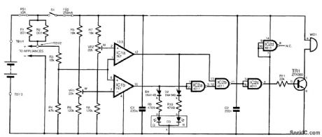
This system is basically an ammeter with a tricolor LED readout in place of a conventional meter. In this system, the tricolor LED shows green for a low demand, yellow for a medium one (acceptable for a temporary heavy load, such as a water pump), and red to indicate excessive use and the need to switch appliances off right away. When red shows, an audible signal is also given. The circuit is built in a small metal box, with the LED mounted on the front panel. A piece of terminal block inside is used to make the connections to the external system.
This circuit must not be used in installations using more than 10A. Having said that, though, the values at which the colors operate are freely adjustable. In the prototype unit, a current below 2A was judged to be low; one between 2 and 4A, medium; and one more than 4A, high. With these criteria, by keeping green, at least 20 hours of operation would be obtained from a standard 60-Ah battery. (View)
View full Circuit Diagram | Comments | Reading(1235)
AXIS_CROSSING_DETECTOR
Published:2009/7/16 20:31:00 Author:Jessie
Used in weak-signal detectors and in theoretical studies of noise.Samples time intervals between positive-going and negative going zero crossings, to establish un interval gate whose width equals time interval of desired weak signal. Output goes to cro for viewing of interval gate.-A. J. Rainal, Digital Measurement Axis-Crossing Intervals,Electronics, 33:23, p 88-91. (View)
View full Circuit Diagram | Comments | Reading(813)
METER_INDICATOR_FOR_CRYSTAL_ACTIVITY_TESTER
Published:2009/7/12 23:50:00 Author:May
A meter can be added as shown, replacing the LED in the original circuit. The meter movement should be a 0- to 1-mA type. (View)
View full Circuit Diagram | Comments | Reading(867)
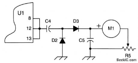
CRYSTAL_ACTIVITY_TESTER
Published:2009/7/12 23:47:00 Author:May
U1 is a 74LS00 quad two-input NAND-gate logic chip.The bo LS version was selected because ofits low current requirement Two of its internal gates are connected as inverters and,In conjunction with R1,R2,and C1,form a crystal oscillator when a crystai is connected between J1 and J2 The third gate,also connected as an inverter,is used as a buffer to provide RF at the crystalfrequency from pin 11,through isolation capacitor C3 and high-pass filter R4 and C6,to J3 so that the crystal frequency can bemonitored by an external-frequency counter The fourth gate,also connected as an inverter-buffer,provides RF at the crystal frequency from puts 8,12,and 13 connected in parallel The RF is fed through isolation capacitor C4 to voltage-doubling rectifiers D2 and D3,and the resulting dc voltage is filtered by C5 and provides a positive bias to the base of Q1,an NPN transistor,which is normally cut off.Q1 goes into conduction, and its collector current flows through LED D1 and R3 in serles,both forming the collector load circuit. The greater the activity of the crystal, the higher the positive bias on the base of Q1 will be, and the higher its collector current will be. This current illuminates D1, and its relative brightness is indicative of the level of crystal activity. (View)
View full Circuit Diagram | Comments | Reading(2726)
VOLTAGE_DIVIDER
Published:2009/7/16 20:19:00 Author:Jessie
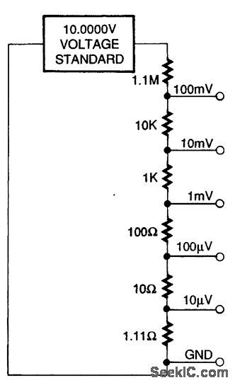
This divider will produce low dc voltages from a 10-V supply. The resistor values can be scaled proportionally for other requirements. (View)
View full Circuit Diagram | Comments | Reading(985)
BROADBAND_RF_TESTER
Published:2009/7/16 20:18:00 Author:Jessie

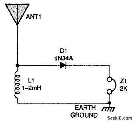
This circuit is useful for crystal radio experimenters for evaluating an antenna and ground setup If you hear some signals, a crystal set will probably work with the antenna and ground. (View)
View full Circuit Diagram | Comments | Reading(1113)
SIGNAL_TRACER
Published:2009/7/16 20:16:00 Author:Jessie
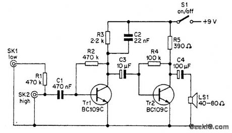
The signal tracer has good sensitivity, so it can be used for any normal type of audio signal tracing. The circuit provides AM demodulation, and the signal tracer can therefore be used for IF and RF testing on AM radios, provided that a suitably strong antenna signal is available. The unit has an integral loudspeaker, and although the maximum output power is only a few tens of milliwatts, the volume level obtained is more than adequate for this application. If preferred, though, the loudspeaker can be replaced by an earpiece or headphones. Low-, medium-, and high-impedance headphones are all suitable for use with the unit. (View)
View full Circuit Diagram | Comments | Reading(0)
ELECTRONIC_STETHOSCOPE
Published:2009/7/16 20:15:00 Author:Jessie
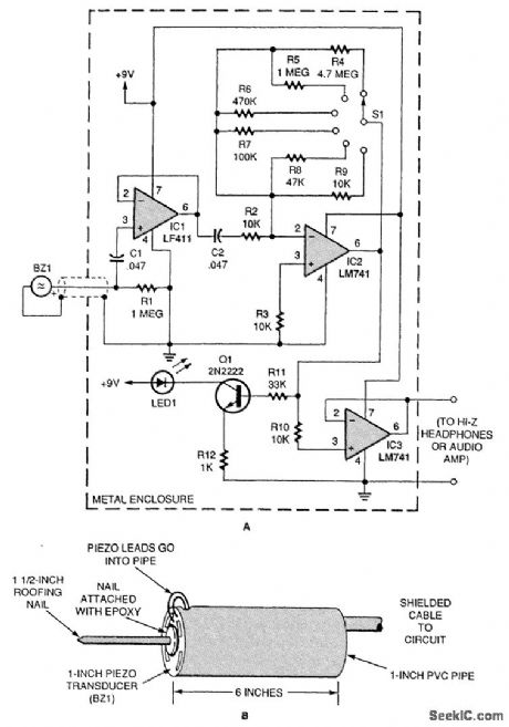
Most electronic stethoscope circuits feature a microphone assembly. Here's one based on a piezo disk used as the transducer. Using 5-min epoxy, glue a roofing nail to the center of the top side of a piezo disk. Be generous with the epoxy, and lay a bead over the top of the nail head. Later, epoxy the outer rim of the backside of the disk to a 1-in diameter PVC pipe roughly 6 in in length, which will serve as a handle. Attach a shielded cable from the piezo-disk leads and secure them in place. The piezo disk's signal is coupled by the cable to IC1, an LF411 FET op amp configured as a buffer. The LF411's output is coupled to IC2, an LM741 op amp configured for high gain. Resistors R4 to R9 set the gain via a rotary switch, but a potentiometer could be used instead. The amp's output goes to both IC3 (a final buffer stage) and Q1 (an MPS7965 general-purpose NPN transistor). The output of the final buffer IC3, an LM741, is connected to high-impedance headphones or a small LM386-based audio amplifier. Power is supplied by two 9-V batteries configured as a split supply. (View)
View full Circuit Diagram | Comments | Reading(908)
10_INTERVAL_TIMER
Published:2009/7/12 23:45:00 Author:May
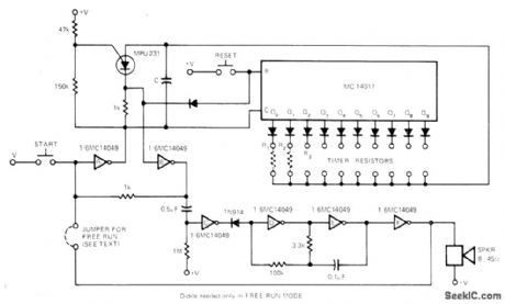
Ten independently predetermined time intervals run in sequence, with audible beep at end of each interval. Timer holds after each interval until start button is pressed to initiate next interval. If jumper is inserted, succeeding intervals start automatically. Values of R1-R9 and C determine time intervals. If same time is used for more than one step, diode outputs of those steps may be tied together to use same resistor. Supply can be in range of 5 to 18 V. Current drain is Iess than 100 μA, but increases to 40 mA during beep. Reset button can be depressed at any time, to restart timing at first intenral.-T. Henry, Ten Step Sequential Interval Timer, EDN Magazine, March 20, 1974, p 78 and 80. (View)
View full Circuit Diagram | Comments | Reading(2595)
| Pages:38/101 At 202122232425262728293031323334353637383940Under 20 |
Circuit Categories
power supply circuit
Amplifier Circuit
Basic Circuit
LED and Light Circuit
Sensor Circuit
Signal Processing
Electrical Equipment Circuit
Control Circuit
Remote Control Circuit
A/D-D/A Converter Circuit
Audio Circuit
Measuring and Test Circuit
Communication Circuit
Computer-Related Circuit
555 Circuit
Automotive Circuit
Repairing Circuit