
Measuring and Test Circuit
Index 39
1_h_HOUSEHOLD_TIMER
Published:2009/7/12 23:43:00 Author:May
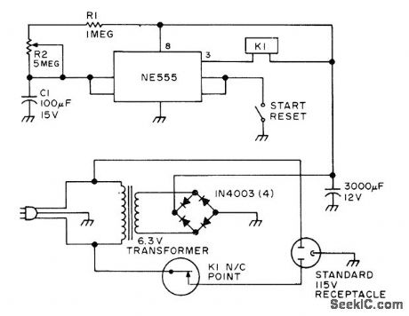
NE555 timer circuit turns off television set or other device at any desired time up to about 1 h after start switch is closed. Use IRC MR312C relay having coil resistance of 212 ohms, or other 12-V relay drawing less than 200 mA. With values shown, R2 gives time delay range of 3 to 58 min. For other ranges, change values of R2 and C1. Clockwise from top, pins on NE555 are 8,3, 4, 2, 1, 7, and 6.-P. C. Walton, Build This $5 Timer, 73 Magazine, Jan. 1976, p 129. (View)
View full Circuit Diagram | Comments | Reading(1076)
DIGITAL_VOLTMETER_CIRCUIT
Published:2009/7/16 21:14:00 Author:Jessie
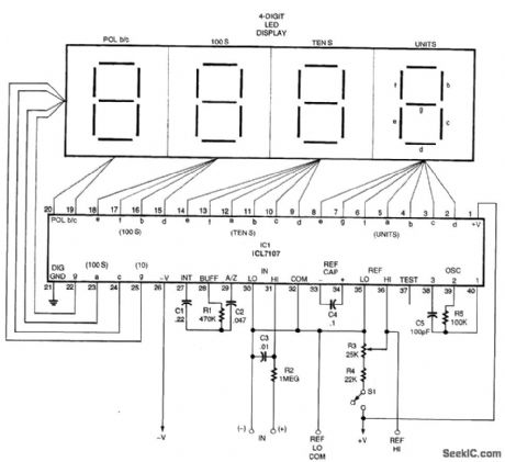
A basic digital voltmeter circuit using the Harris Semiconductor ICL7107 is shown. It has a 2-V range. Calibration consists of applying a known voltage of 1.2 V to the input and adjusting R3 for a correct reading on the display. Supply is ±5 V, and S1 selects either the supply voltage or an external reference. (View)
View full Circuit Diagram | Comments | Reading(5670)
MICROSECONDS_TO_HOURS_1
Published:2009/7/12 23:21:00 Author:May

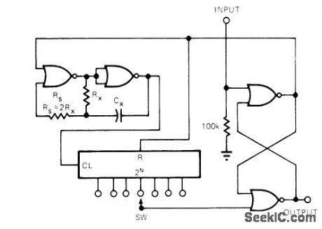
Simple CMOS circuit serves as time-delay switch and generalpurpose timer. Gated oscillator and latch are obtained from CD4001 quad two-input NOR gate, and 14-stage counter uses CD4020. TON is function of oscillator frequency as determined by RXCX and proper 2N output from counter. Pulse applied to latch input enables oscillator and counter. Latch output remains high until counter resets latch at end of count selected by switch. Further decoding is required for count or time variations finer than power of 2.-J.Chin, Low-Power Counter is Programmable over Wide Range, EDN Magazine, March 20, 1974, p 83. (View)
View full Circuit Diagram | Comments | Reading(2691)
AC_LINE_VOLTAGE_MONITOR
Published:2009/7/16 21:09:00 Author:Jessie
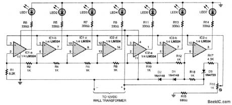
This figure shows the schematic of the ac line-voltage monitor circuit. The circuit receives 12 Vdc from a wall transformer. The circuit is centered around two quad LM324 op-amp ICs (IC1 and IC2) that receive regulated operating power from a clamped portion of the dc supply provided by a 5.1-V zener diode, D3. The op amps drive an LED bar graph, consisting of LED1 through LED7. The op amps receive an adjustable reference voltage from the center contact of potentiometer R16 and an input voltage from the voltage divider, consisting of resistors R1, R2, R4, R6, R8, R10, R12, and R18. Those resistor values were chosen so that the op-amp outputs sequentially turn on and light the LEDs as the ac line voltage, or one-tenth of it, varies from 100 to 132 V. Potentiometer R16 sets the midpoint of the LED bar graph-usually 118 V-which can be shifted, if you like. (View)
View full Circuit Diagram | Comments | Reading(5592)
DUMMY_LOAD_AND_DETECTOR
Published:2009/7/12 23:08:00 Author:May
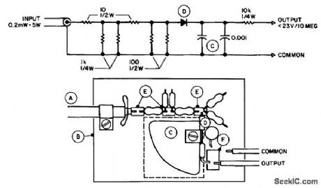
Two 100-Ω, 1/2-W resistors in parallel connected across a 50-Ω cable with near-zero lead lengths will be very close to a 50-Ω termination with the SWR less than 1.1:1. However, adding the diode introduces capacitor loading that results in an SWR of 1.5:1 or more. In the circuit, the components on the 2-dB resistor pad preceding the diode/load compensate for this, as they are tailored to reduce the SWR to less than 1.1: 1. Although the power capability of this assembly is 5 W, forced-air cooling is required at the higher power levels, depending on the measurement period.Schematic and layout of the dummy-load/detector assembly: A. Input, 1 ft RG-58/U. Fan out braid on connectink end, twist in two segments, and solder to PC board with minimum lead lengths. B. Base, 3 in2 ×in×1/16 in PCB. C. Capacitor-90° circular sector, 1 in radius, 0.21-in-thick Reynolds sheet aluminum. Surface polish with 220-grit sandpaper to remove burrs. Dielectric, 2.7-mil polyethylene (Ziploc heavy-duty freezer bag). Feed through 2-56 screw with a plastic insulator on the back side. Hole is reamed on both sides with a large drill to prevent shorting to the foil. D. Peak readout diode, 1N34A selected to have a reserve resistance of less than 5 MΩ (RS 276-1123). E. Component tie-down pads, 1/4 in1/×8 in×1/16 in glass-epoxy PC board. Cemented to base with clear household cement (Elmer's). F. Output tie-down pad 3/8 in1×/4 in×1/16 in PC board. (View)
View full Circuit Diagram | Comments | Reading(1104)
SEQUENTIAL_TIMER_1
Published:2009/7/12 23:07:00 Author:May

Second Exar XR-2242 long-range timer is triggered when first timer completes its cycle, length of which is equal to 128R1C1. Output of second timerthus stays high for T1 = 128R1C1 after trigger is applied, then goes low for duration T2 =128R2C2 corresponding to timing interval of unit 2. Circuit then reverts to rest state.- Timer Data Book, Exar Integrated Systems, Sunnyvale, CA, 1978, p 19-22. (View)
View full Circuit Diagram | Comments | Reading(0)
05333_136_s_WITH_LINE_FREOUENCY_ACCU_RACY
Published:2009/7/12 22:57:00 Author:May
Provides time delays in selected increments of 0.5333 s with accuracy essentially that of AClinefrequency. IC1 develops 120pulses per second having 100-μs width at pins 4 and 6 for each zero crossing of line. First six stages of IC2 determine basic timing period 1T, These stages produce pulse train with periodicity of 0.5333 s at input of seventh counter stage. Binary-or-dered output signals are available at outputs ah for 1T, 2T, 4T,.. 1287. Thus, for delay of 1 min (about 1127), use 64T + 32T, + 16T with AND-gate programming interconnections e-E, f-F, and g-G. Tie all unused AND-gate inputs to VDD bus.-A. C. N. Sheng, Line-Operated Timer Couples High Apeuracies with Long Time Delays, EDN Magazine, Jan. 5, 1976, p 37-40. (View)
View full Circuit Diagram | Comments | Reading(1014)
DIGITAL_COUNTER_CIRCUIT
Published:2009/7/12 22:56:00 Author:May
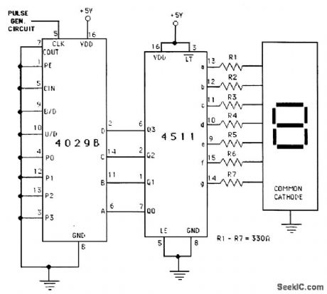
This circuit shows how a simple digital counter can be implemented. A CD4029B drives a DC4511 decoder and LED driver. A common-cathode LED display is used. (View)
View full Circuit Diagram | Comments | Reading(3164)
VOLTAGE_CALIBRATOR
Published:2009/7/16 20:54:00 Author:Jessie

A NE555 oscillator drives a regulator to provide a regulated square-wave voltage to a voltage divider. The output is 1 to 5V p-p in 1-V steps. (View)
View full Circuit Diagram | Comments | Reading(1103)
DELUXE_RADAR_DETECTOR_
Published:2009/7/16 22:10:00 Author:Jessie
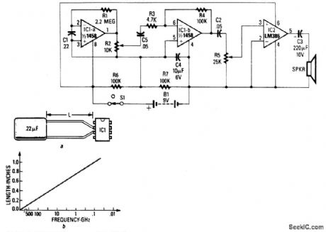
This simple radar detector includes an audio amplifier for driving a loud speaker. As in Fig. 69-1, it uses an op amp as a detector of microwave signals. (View)
View full Circuit Diagram | Comments | Reading(4891)
4_WAY_LOGIC_PROBE
Published:2009/7/16 21:44:00 Author:Jessie
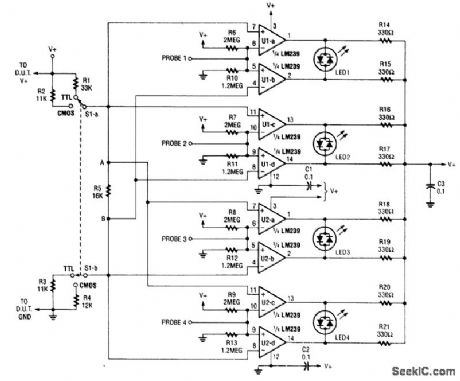
This logic probe has four channels and uses two IF quad comparators to drive four bicolor LEDs. S1 and S1B program the comparator trip levels for TTL and CMOS. R6 through R13 bias the probe inputs to prevent the probe from indicating a HIGH for an open circuit. An open circuit will produce an OFF indication on the LED. The LEDs will indicate one color for high, the other color for low, and intermediate colors for pulsing (assuming a duty cycle between 30 and 70%). The color that corresponds to HIGH or Low depends on how you connect the LEDs. (View)
View full Circuit Diagram | Comments | Reading(1628)
ELECTRET_MIKE_CIRCUIT
Published:2009/7/16 21:41:00 Author:Jessie
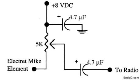
This circuit shows how to power an electret microphone. The 5-kΩ potentiometer acts as a gain control. (View)
View full Circuit Diagram | Comments | Reading(1020)
BLOOD_OXYGEN_MEASUREMENT
Published:2009/7/16 21:39:00 Author:Jessie

An oximeter measures the amount of oxygen in your blood by shining light through some part of your body-traditionally the earlobe, nowadays often the finger-and comparing the transmission of two different wavelengths, 800 nm (in the near infrared) and 640 nrn (bright red). If they're about the same, your oxygen is very low; if your blood is well oxygenated, the 640-nm transrnission will be much higher. The light sources are LEDs, and the detector is a silicon photodiode or phototransistor. (View)
View full Circuit Diagram | Comments | Reading(1529)
TWO_FUNCTION_CONTROLLER
Published:2009/7/12 22:32:00 Author:May
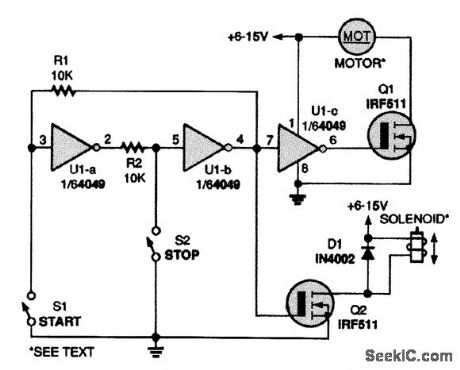
This two-function controller operates a motor when started, then energizes a solenoid, relay,etc., when stopped. (View)
View full Circuit Diagram | Comments | Reading(997)
FOUR_OUTPUT_CONTROLLER
Published:2009/7/12 22:31:00 Author:May
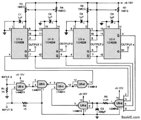
This controller offers up to four timed outputs that can be used to operate motors, air valves, solenoids, relays, etc. The timer sections are cascaded so that as one timer times out, it triggers the next timer, and so on, until the last timer times out. The intended application for the controller required a two-sensor input that would start only when both inputs occur simultaneously. Note, however, that the start-signal logic could be modified to accommodate a combination of any number of input sensors, or even a single switch closure. The controller also includes an inhibit circuit that keeps the sequence from restarting before a cycle is completed. (View)
View full Circuit Diagram | Comments | Reading(1230)
TEN_STEP_COUNTER_FOR_CONTROLLERS
Published:2009/7/12 22:29:00 Author:May
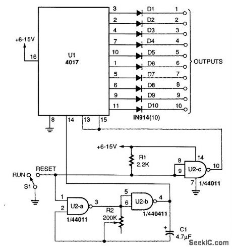
A 4017 divide-by-10 counter IC is the heart of this simple 10-output controller circuit. Two gates of a 4011 quad two-input NAND gate IC are connected in an astable oscillator circuit to clock the divide-by-10 counter U1. The step time is set by R5. With the RUN/RESET switch in the RUN position, U1 takes 10 equal steps and then stops. Momentarily switching S1 to RESET starts the cycle over (View)
View full Circuit Diagram | Comments | Reading(3087)
PULSE_AMPLITUDE_MEASUREMENT
Published:2009/7/16 22:57:00 Author:Jessie
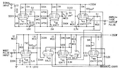
Produces pulse whose width is linearly related to se looted portion of input signal. V42 is Schmitt trigger. V46 is flip-flop controlled by output from mognetron-beam switching tube (MBST) for selecting desired sample of signal. Output pulse width is sampled and measured by counter.-J. F. Lyons, Jr., Analyzing Multipath Delay in Communications Studies, Electronics, 32:36, p 52-55. (View)
View full Circuit Diagram | Comments | Reading(845)
VOLTAGE_LIMIT_DETECTOR
Published:2009/7/16 22:36:00 Author:Jessie
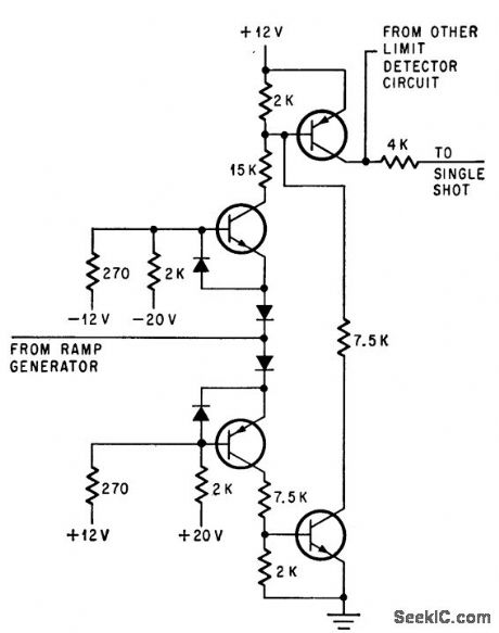
Consists of two voltage dividers that set the levels between which ramp generators should remain in roster that shows computer memory performance under marginal drive currents by plot ting schmoo curves. Npn transistors ore 2N706, pnp transistors are 2N1132, and diodes are 1N921.-J. E. Gersbach, The Great Schmoo Plot: Testing Memories Automatically, Electronics, 39:15, p. 127-134. (View)
View full Circuit Diagram | Comments | Reading(1237)
10_s_TIMER
Published:2009/7/12 22:09:00 Author:May
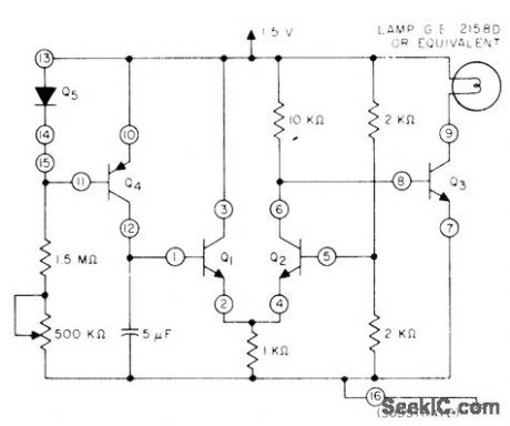
CA3096 transistor array provides all needed active devices, 5-μF capacitor charges through Q4 until it turns on bistable switch Q1-Q2, which then triggers Q3 to deliver current to lamp load to indicate end of timing interval.- Circuit ldeas for RCA Linear ICs, RCA Solid State Division, Somerville, NJ, 1977, p8.
(View)
View full Circuit Diagram | Comments | Reading(972)
CONSTANT_OFF_TIME_REGULATOR_WITH_FREQUENCY_COMPENSATION
Published:2009/7/17 1:39:00 Author:Jessie
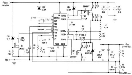
Constant off-time switching regulators offer several advantages over constant-frequency designs The only potential problem is that the switching frequency Increases with nsmg input voltage In designs that have large ratios of the high line to low-line supply voltage,this frequency shift can get quite large As a result,the switching losses can become excesslve at high input voltages To offset this problem,the simple circuit shown detects the high input voltage condition and lowers the switching frequency to keep switching losses under control The frequency-shift circuit consists of D3,R8,Q1,and C12 When Vin exceeds the zener voltage plus the FET threshold,Q1 turns on and adds an extra timing capacitor(C12) in parallel with the timing capacitor (C10) This increases the off-time,lowering the frequency. (View)
View full Circuit Diagram | Comments | Reading(1645)
| Pages:39/101 At 202122232425262728293031323334353637383940Under 20 |
Circuit Categories
power supply circuit
Amplifier Circuit
Basic Circuit
LED and Light Circuit
Sensor Circuit
Signal Processing
Electrical Equipment Circuit
Control Circuit
Remote Control Circuit
A/D-D/A Converter Circuit
Audio Circuit
Measuring and Test Circuit
Communication Circuit
Computer-Related Circuit
555 Circuit
Automotive Circuit
Repairing Circuit