
Measuring and Test Circuit
Index 37
BENCH_POWER_SUPPLY_METER
Published:2009/7/16 4:04:00 Author:Jessie
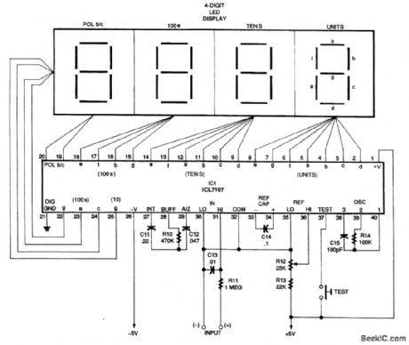
The heart of the digital meter is the Harris ICL7107 A/D converter. The 7107 contains all the active devices needed to construct the voltmeter. These include the segment decoders and LED display drivers. The optional push-button switch connected to pin 37 of the ICL7107 permits the display to be tested. When that pin is connected to +5 V, the display will indicate -1888, testing all the segments. If a liquid-crystal display is preferred, substitute an ICL7106CPL for the 7107. All pin connections will be the same, except that pin 21 will become the backplane instead of the digital ground. (View)
View full Circuit Diagram | Comments | Reading(7698)
PLL_LOCK_DETECTOR
Published:2009/7/13 3:46:00 Author:May
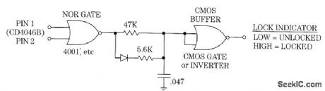
When the loop is locked, the waveforms at pins 1 and 2 of CD4046B are almost identical, differing only in polarity. This holds the output of the NOR gate low. When the loop is not locked, the output of the NOR gate is a series of pulses. This charges the 0.047-μF capacitor, and causes a low output from the CMOS buffer. (View)
View full Circuit Diagram | Comments | Reading(1158)
HV_STATIC_DETECTOR
Published:2009/7/13 3:45:00 Author:May
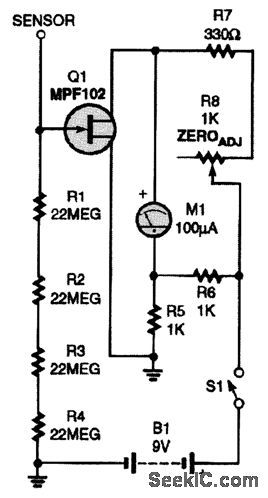
One leg of a Wheatstone bridge is replaced by an MPF102 N-channel JFET. The JFET's high gate input impedance turns the simple bridge circuit into a very sensitive high-voltage static detector.The JFET's gate is tied to ground through four 22-MΩ resistors. A 1- to 2-in piece of solid-copper wire is connected directly to the JFET's gate and serves as the input sensor. With the sensor clear, adjust R8 for a zero meter reading. Run a comb through your hair and move it toward the sensor.The meter should go off the scale. Place the staticsensor next to your computer or any static sensitive equipment and take special notice when the meter moves. (View)
View full Circuit Diagram | Comments | Reading(2428)
MISSING_PULSE_DETECTOR
Published:2009/7/13 3:44:00 Author:May
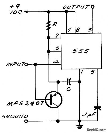
A missing-pulse detector is a circuit whose output is triggered only when there is a loss of signal at its input. In the circuit shown, the 555 timer IC is configured as a one-shot multivibrator that produces a pulse whose width is determined by the value of resistance R and capacitance C, shown in the schematic. The values for those parts can be calculated by using the formula T=1.1RC. Select values that make the output pulses about twice as wide as the input trigger pulses from the control line. As long as there is a steady stream of input trigger pulses, the 555 will output a logic high. If there is only one input pulse period, the 555 will time out and its output will go logic low until the next trigger pulse arrives. The logic low at the 555 output can trigger an alarm, a time recorder, a counter, or any other device. (View)
View full Circuit Diagram | Comments | Reading(0)
INVERTED_VEE_ANTENNA
Published:2009/7/13 3:36:00 Author:May
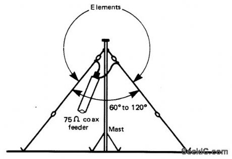
The inverted vee antenna is widely used by SWLs and radio amateurs. It has the advantage of needing only one support and can be fit into somewhat smaller spaces in some instances. A balurt having a 1:1 impedance designed for 50Ω can be installed at the feed point for improved performance, if desired.
(View)
View full Circuit Diagram | Comments | Reading(1136)
ANTENNA_NOISE_BRIDGE_DETECTOR
Published:2009/7/13 3:35:00 Author:May

The circuit is illustrated in the figure. The noise output from your antenna noise bridge is applied though a coax jumper cable to J1, an SO-239. This noise, which usually will peak slightly below 1.0 V, is broadband white noise and is fed though C1, a 100-pF capacitor, to a pair of small-signal diodes connected as a rectifier/voltage doubler. The rectified dc voltage, filtered by C3, an 0.1-μF disk capacitor, is then applied to the base of a small-signal NPN transistor (Q1), which serves as a meter amplifier. Meter M1 is a 200-μA meter. It monitors collector current through Q1. On/off switch S2 is mounted on the GAIN control, which, in series with R3, forms a voltage divider across battery BT1, a 9-V battery, which powers this instrument. The GAIN control is wired so that the wiper travels from the end of R3 to ground as the krtob is rotated clockwise. This sets the emitter bias and the point at which Q1 will go into conduction as rectified noise voltage is applied to the base of Q1. The current drain from the battery is approximately 8 pA with no input, increasing to slightly over 200 μA with the meter at full scale. With such low current drain, an alkaline battery should last for years, even if you forget to turn the instrument off! This instrument covers the range from below 40 m to above 10 min two bands: 40 and 30 m, and 20-17-15-12-10 m. Bandswitch S1, an SPDT toggle or slide switch, selects the frequency range. The tuning capacitor C2 is a small 150-pF air variable. (View)
View full Circuit Diagram | Comments | Reading(1632)
THREE_RANGE_LIGHT_METER
Published:2009/7/13 3:34:00 Author:May
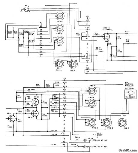
Uses probe containing Clairex 905HN light-dependent resistance element, connected to DC differential amplifier driving meter having specially calibrated scale. Article gives calibration procedure. Switching circuit provides constant check on voltage of 22.5-V battery. If 4.5-V battery is low,full-scale adjustment cannot be made Resistors having values specified in article are connected in turn to terminals of photocell jack P1 for calibration that gives linear scale reading.-J.L. Mills, Jr., Light Right?-Do-It-Yourself Photo Exposure Meter, 73 Magazine, Sept.1978,p 204-206 and 208-211. (View)
View full Circuit Diagram | Comments | Reading(923)
SIMPLE_POLARITY_INDICATOR
Published:2009/7/16 4:00:00 Author:Jessie
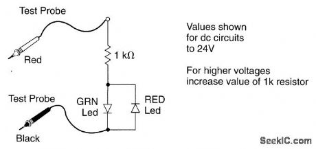
Use this circuit to determine the polarity of low-voltage dc circuits. If the green LED lights, the red probe is positive. If the red lights, the red probe is negative. (View)
View full Circuit Diagram | Comments | Reading(1358)
LED_SWR_INDICATOR_CIRCUIT
Published:2009/7/16 3:59:00 Author:Jessie


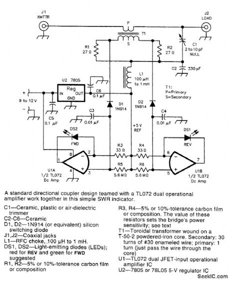
D1 and D2 act as half-wave diode detectors for the forward and reverse voltages. In traditional SWR-meter circuits, the output of these detectors feeds a panel meter via a forward/reflected switch and a scaling resistor, which typically provides the detector diodes with a load on the order of 25 kΩ. This relatively low load impedance limits the diodes' performance at low power levels because it causes their forward voltage drop to be higher than the sampled RF voltages to be detected. To use LEDs (DS1 and DS2) as indicators, some sort of dc amplifier was needed. Operational amplifiers were used because their high input impedance lets us load the diodes so lightly that their detection range can extend down to about 50 mV. U1A and U1B, halves of a TL072 dual JFET-input op amp, do the dc amplification. The dc voltage developed by each detector is presented to its op amp across a 5.6-MΩ resistor. Each op amp operates at a voltage gain of 1 (unity), but provides enough current gain to drive an LED and to cause a matching voltage to appear across R3. To provide each half of U1 with split (positive and negative) power supplies in environments in which only single-polarity, negative-ground supplies are typical, it was necessary to provide an artificial ground. U2 provides a stiffly regulated dc voltage between ground and the positive supply. (Note that the bridge circuit's dc reference is also set to +5V because the RE-grounded end of L1, which is connected to dc ground in traditional directional-watt meter circuits, is also connected to the +5-V supply provided by U2.) The overall sensitivity of the circuit can be adjusted to match the power level expected by changing the values of R3 and R4 to drive the LEDs with an appropriate current level. If you use different LEDs or want to use the bridge at a different power level, you may want to adjust these resistor values ac-cording to the formula R3 and R4 (ohms)=√P0×50/30×If(LED) ,where P0 is the transmitter power in watts, 50 is the system impedance in ohms, 30 is T1's turns ratio, and If(LED) is the current level (in amperes) that produces the LED brightness you need. With the resistor values chosen to light the FED LED (DS2) brightly, the REV LED (DS1) will be easily visible at SWRs around 2:1, allowing no-guess SWR dipping with tuner adjustment. (View)
View full Circuit Diagram | Comments | Reading(2982)
CONVEYOR_MONITOR
Published:2009/7/13 3:23:00 Author:May
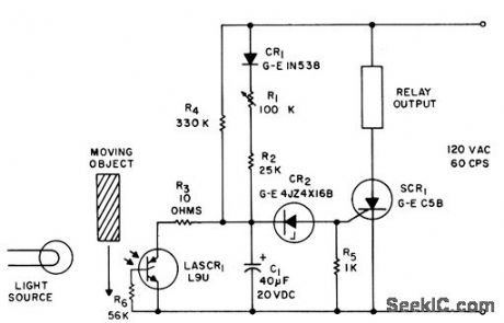


Will shut down conveyor line rapidly to prevent catastrophic jam, while ignoring small self-clearing pileups. Each time light beam is interrupted, light-activated scr is briely commutated by a-c line. C1 starts to charge but is shorted to zero as light is restored. If light path is blocked more than a few millisec, C1 continues to charge and fires SCR1 to stop conveyor.- Silicon Controlled Rectifier Manual, Third Edition, General Electric Co.1964, p 214. (View)
View full Circuit Diagram | Comments | Reading(992)
CHART_RECORDER_RANGE_EXTENDER
Published:2009/7/16 5:41:00 Author:Jessie

The circuit diagram shown was designed to adapt a laboratory chart recorder with a 100-mV in-put for full-scale deflection so that it will accept input voltages of 1V, 2V, 5V, or 10V at the flick of a switch. The op amp (IC1) is configured as an inverting amplifier whose feedback resistance is much less than the input resistance (R1); therefore, the output voltage will be a fraction of the input signal. Range switch S1 selects among four different feedback resistors, which consist of fixed metal-film resistors and a 20-turn cermet trimmer, which is adjusted to produce 100 mV output at the selected input voltage range. In practice, VR2 should be adjusted to 100 mV output at 2V input. The other ranges are set up in the same manner. (View)
View full Circuit Diagram | Comments | Reading(1440)
FOUR_CELL_TO_5_VDC_CONVERTER
Published:2009/7/13 2:54:00 Author:May
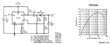
Generating a regulated 5-V output frorrt a four-cell NiCd battery pack requires step-down opera-tion when the battery voltage is above 5 V (fully charged pack at 6 V) and step-up operation when the battery voltage drops from 5 V to 3.6 V during discharge. The LT1373 converter circuit shown achieves up to 83 percent efficiency at high current (100- to 200-mA range), better than a flyback approach. The 250-kHz switching frequency minimizes inductor values, and both 33-μH inductors are wound on the same core, requiring less board area. With a quiescent current of I mA typically, the LT1373 offers high efficiency at high frequency, extending the battery lifetime in applications. (View)
View full Circuit Diagram | Comments | Reading(989)
BIKE_SPEEDOMETER_CIRCUIT
Published:2009/7/16 5:39:00 Author:Jessie
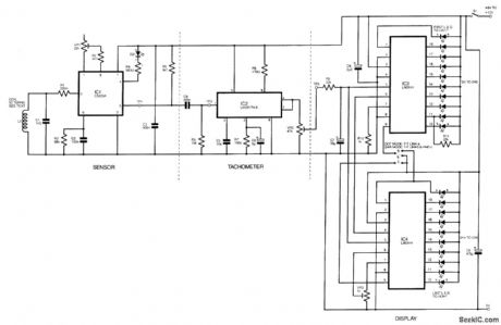
The proximity detector senses the passing of the PC board pieces as the wheel rotates, providing an output signal, which has a clean transition between high and low voltage levels, and is ideal for triggering counting or processing circuits. Next is the frequency-to-voltage converter, and, because a reasonable degree of accuracy is required, the LM2917N-8 IC has been chosen. The output from this IC is fed to two bar-graph ICs, which drive a 20-LED display. (View)
View full Circuit Diagram | Comments | Reading(4721)
20_CHANNEL_DECODER_FOR_AUDIO_TONES
Published:2009/7/13 2:51:00 Author:May
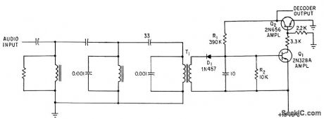


L-C filter in each decoder is tuned to channel tone,with 35-db adjacent-channel rejection.Rectified output of detector D1 drives two-stage d.c amplifier having relay load. Used in Mercury spacecraft command receiver.-R.Elliott,First Details on Mercury Spacecraft Command Receiver,Electronics,36:5,p32-35 (View)
View full Circuit Diagram | Comments | Reading(901)
RIPPLE_ADDER
Published:2009/7/16 5:36:00 Author:Jessie
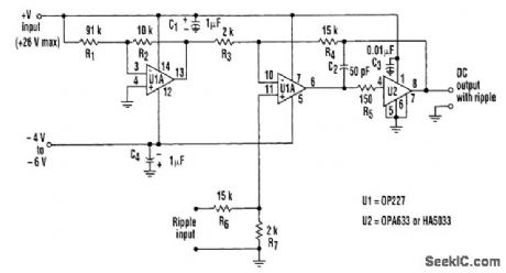
When a device under test needs a dc voltage applied with ripple superimposed, this circuit can handle the task. The power supply for the +V input will need to be set about 20 percent higher than the desired output. The supply should be well regulated, because it directly affects the output volt-age. A function generator set to the desired waveform, amplitude, and frequency must be connected to the ripple input. Because of resistor tolerances, the final voltage adjustments will have to be made by monitoring the output. U2 will drive capacitive loads as long as the dc + peak ac doesn't exceed 200 mA. The frequency response of the ripple adder with a 5-V p-p output ranges from dc to past 100 kHz. R5 and C3 should be located as close as possible to U2. R1 can be altered to change the ratio between the input and output voltages. (View)
View full Circuit Diagram | Comments | Reading(988)
STRIP_CHART_RECORDER_FROM_OLD_COMPUTER_PRINTER
Published:2009/7/16 5:29:00 Author:Jessie
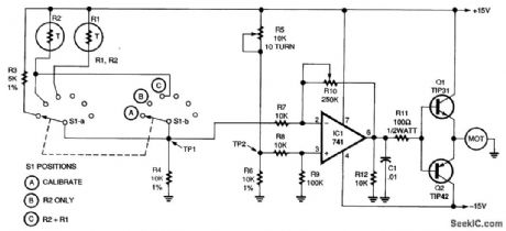
Converting an obsolete computer printer into a strip-chart recorder is both easy and inexpensive. The chart recorder works by comparing the voltage on a potentiometer to the voltage on a temperature-sensing thermistor. The potentiometer is mechanically connected to the printer carriage. A marking pen is also connected to the printer carriage. Any difference in the voltages on the potentiometer and the temperature sensor causes an op amp to attempt to bring the voltages back into balance. In the course of this, the print-head carriage is moved left or right, thereby causing a mark on the paper. A standard 741 op amp is used as a comparator. The comparator monitors the voltages at the junctions, marked TP1 and TP2. The op amp compares the voltages from the two networks at its inputs (pins 2 and 3). When the voltages are identical, the op amp's output (pin 6) is zero, so neither driver transistor (Q1 and Q2) turns on; therefore, the motor does not turn. But if thermistor R2's resistance changes because of a change in air temperature, a new voltage occurs at the op amp's inverting input (pin 2). For example, assume that R2 decreases.
The pin 2 voltage then increases, so the op amp's output swings negative, thereby biasing Q2 on. That in turn starts the motor, which moves the carriage left or right. Potentiometer R5 is also coupled to the carriage, so, as the carriage moves, R5's wiper moves, thereby varying the voltage on the noninverting input of IC1. When the op amp's input voltages become equal, the output goes to zero, both transistors turn off, and so does the motor. Now the circuit remains quiescent until the temperature changes again. (View)
View full Circuit Diagram | Comments | Reading(2436)
FREQUENCY_RESPONSE_TESTER
Published:2009/7/16 5:26:00 Author:Jessie
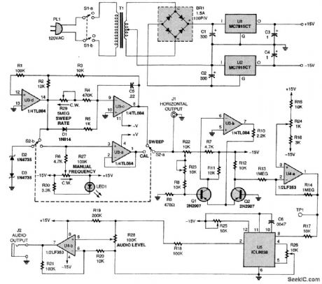
The two quad op-amp sections, U3-c and U3-d, are configured as a linear ramp generator. With switch S2 in the SWEEP position, as shown, the output of U3-d is low. Zener diodes D2 and D3 limit that output to about -7V, which is the 6.2-V reverse drop across D3 plus the forward drop of D2. The internal short-circuit protection of the op amp limits the zener current to several milliamperes. Because the output of U3-d is negative, integrator U3-c generates a linear ramp in a positive direction, at a rate determined by the resistance of R4 and R29 and the capacitance of C5. A portion of that output is fed back to the noninverting input of U3-d. Because U3-d is basically operating as a comparator with its inverting input grounded, its output will switch positive as soon as its noninverting input crosses zero volts. The overall effect is to produce a saw tooth waveform with an amplitude of over 10-V p-p. That is more than sufficient for just about any scope's horizontal input. Next, the linear ramp under-goes a series of level and offset adjustments via resistors R7, R8, R9, R22, and R23, and is then applied to the base of Q1. The emitter-coupled transistors, Q1 and Q2, in combination with U3-b, produce an antilog transfer function. The output at the collector of Q2 will be logarithmic with respect to the in-put, yielding a one-decade voltage differential for every few volts of input. Next, U4-a inverts the polarity of the signal, so that it starts high and ends low. That is necessary because the output frequency of the 8038 function generator, U5, is inversely proportionalto its input voltage. The ICL8038 function generator produces constant-amplitude sine waves, as well as triangle- and square-wave outputs, from 20 Hz through 20 kHz. Also, its output frequency is nearly a perfect inverse proportional to its in-put voltage, so driving its input with a logarithmic sweep circuit will produce the balanced, three-decade frequency sweep. The sine-wave output from U5 is fed to the voltage divider made up of R18 and R19, which restores the dc offset to zero. The voltage-divider output is then applied to potentiometer R28 for output-level control, and is subsequently routed to U4-b for a boost in both amplitude- and current-drive capability. The output can range from 0 to over 10 V p-p. (View)
View full Circuit Diagram | Comments | Reading(3949)
LED_PEAK_INDICATOR
Published:2009/7/16 4:53:00 Author:Jessie
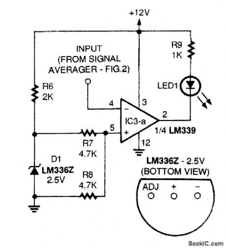
The voltage divider consisting of resistor R6 and 2.5-V precision voltage reference IC2 forms a precision voltage reference whose voltage is divided in half at the junction of resistors R7 and R8.This places a reference voltage of 1.25V at the comparator noninverting input. Whenever the inverting input voltage exceeds the reference voltage, the output will be connected to ground internally, and LED1 will light. With the input of this circuit connected to the output of the averager circuit, the LED will flash on whenever the audio input exceeds the level set with gain potentiometer R2. Adjust R2 by applying a maximum level signal to the input of the averager, and then reduce the level slightly to allow for headroom. With the input level now set, adjust R2 until the peak LED just turns on. (View)
View full Circuit Diagram | Comments | Reading(1689)
DECIBEL_METER
Published:2009/7/16 4:50:00 Author:Jessie
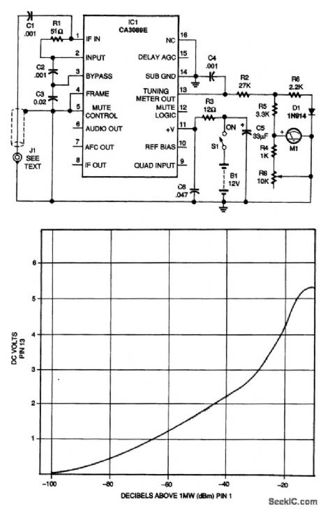
The circuit consists essentially of IC1, the CA3089E, a 0-to 100-μA meter M1, on-off switch S1, a few resistors and capacitors, and a diode. The graph shows the plot of dc volts out of METER OUT, pin 13 of IC1 (33 kΩ to ground), vs. the input signal in microvolts on IF IN 1, pin converted to decibels above 1 mW. IC1 detects the signal level and generates a nearly logarithmic dc output. To linearize the high end of this curve, diode D1 and resistor R6 shunt some of the dc as the voltage on pin 13 rises above 3 V. The battery pack, consisting of eight AA alkaline cells, makes the instrument portable and eliminates the possibility of 50/60-Hz hum interfering with the readings. The meter draws only about 16 mA, so battery life will be long. The meter will provide accurate readings as long as the output of the battery pack remains above 8 V. No regulation of this dc is required. (View)
View full Circuit Diagram | Comments | Reading(2364)
6_TO_25_V_INPUT_5_V_125_A_DC_TO_DC_CONVERTER
Published:2009/7/13 2:33:00 Author:May
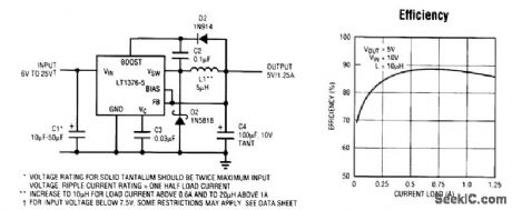
One of the keys to success for many portable devices is small size. In many cases, the requirement for a wide battery supply voltage range and high-current, regulated 5-V output seems incompatible with the size requirement. The 500-kHz LT1376, shown in this circuit, provides a powerful, compact power supply. Operating at such a high frequency permits the use of a very small 5-μH surface-mount inductor and a surface-mount output capacitor. In addition, the intemal switch has just 0.4 Ω of ON resistance, which reduces power loss and boosts efficiency to 88 percent. A special boost pin and circuitry reduces the minimum operating supply voltage in step-down applications. The maximum current rating of the switch is 1.5 A. The input voltage range extends from 6 to 25 V and is well matched for many battery-pack assemblies. The typical supply current is 4 mA, whereas the shutdown current is just 20 μA. (View)
View full Circuit Diagram | Comments | Reading(871)
| Pages:37/101 At 202122232425262728293031323334353637383940Under 20 |
Circuit Categories
power supply circuit
Amplifier Circuit
Basic Circuit
LED and Light Circuit
Sensor Circuit
Signal Processing
Electrical Equipment Circuit
Control Circuit
Remote Control Circuit
A/D-D/A Converter Circuit
Audio Circuit
Measuring and Test Circuit
Communication Circuit
Computer-Related Circuit
555 Circuit
Automotive Circuit
Repairing Circuit