
Measuring and Test Circuit
Index 29
DIFFERENTIAL_INPUTS_GIVE_GROUND
Published:2009/7/15 2:53:00 Author:Jessie
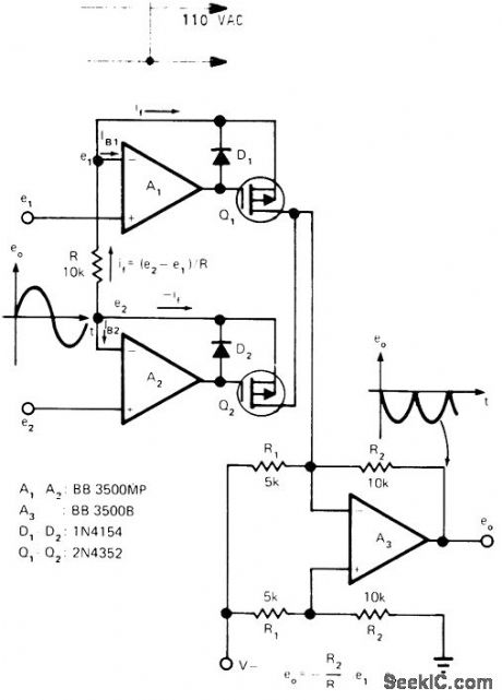
REFERENCED OUTPUT-Circuit consists of differential-input controlled-current rectifying source A1-A2 and level-shifting voltage-to-current converter A3. Feedback current of appropriate polarity is conducted to output opamp, while other feedback current is absorbed. Possible drawbacks are switching offset and bandwidth limitations common to precision rectifiers. Article gives design equations and theory of operation.-J. Graeme, Measure Differential AC Signals Easily with Precision Rectifiers, EDN Magazine, Jan. 20, 1975, p 45-48. (View)
View full Circuit Diagram | Comments | Reading(1156)
AC_PEAKS
Published:2009/7/15 2:52:00 Author:Jessie
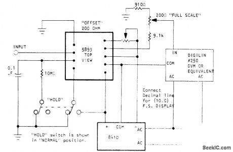
Optical Electronics 5893 peak sense-and-hold analog memory module senses input peaks of AC waveforms and produces smooth DC output voltage for driving 21/2 -digit digital voltmeter. Output of 5893 is divided by about 10 to give 1-V full-scale output for meter. External capacitor used with parallel resistor provides time constant required for steady display on DVM. Response time is 4 s for input change from 10 V to 0 and less than n s for rise from 0 to 10 V. Useful bandwidth is 20 Hz to 2 MHz. HOLD switch is operated when peak reading on meter is to be held several minutes.- Digital Peak Reading AC Voltmeter, Optical Electronics, Tucson, AZ, Application Tip 10259. (View)
View full Circuit Diagram | Comments | Reading(1358)
PHONE_CALL_COUNTER
Published:2009/7/14 8:12:00 Author:May
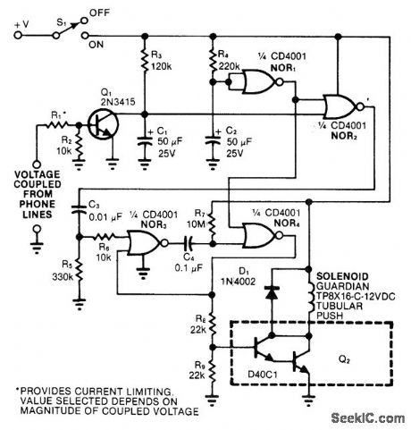
Circuit actuates solenoid that depresses R/S counting key of SR-56 calculator for each interrogation event consisting of sequence of pulse bursts each corresponding to ring of phone. Bursts are separated by 4-s pauses, so circuit includes time delay that prevents actuation of solenoid until line has remained quiescent for more than 5 s after burst. Article includes program that is inserted in calculator to total number of times R/S key is de-pressed. Applications include counting number of telephone calls received while away.-M. Bram, Hardware + Program Makes SR-56 Event Counter, EDN Magazine, Aug. 5, 1978, p 84 and 86. (View)
View full Circuit Diagram | Comments | Reading(0)
DUAL_TIMER
Published:2009/7/14 5:38:00 Author:May
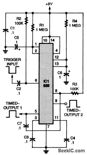
Two are sometimes better than one. This dual timer contains a 556 IC, which contains two 555 timers in one package. (View)
View full Circuit Diagram | Comments | Reading(1097)
DC_VOLTMETER
Published:2009/7/15 2:33:00 Author:Jessie

Opamp connected for closed-loop gain of 100 is used with attenuator network and 100-μA microammeter to serve as general-purpose multirange laboratory voltmeter. Additional full-scale output of ±10 V is provided for driving chart recorder. Low-pass filter R4-R5-C1-C2 prevents amplifier from overloading on large AC input signals while allowing circuit to read DG component. Filter acting with diodes protects amplifier from input overloads up to1000 V.-R. S, Burwen, Simple DC Voltmeter Uses Single Op Amp, EDN/EEE Magazine, Dee. 15, 1971, p 57. (View)
View full Circuit Diagram | Comments | Reading(0)
IR_REMOTE_TESTER
Published:2009/7/14 7:25:00 Author:May
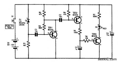
This remote handset tester is very useful and convenient, and could quickly pay for itself by helping to recover faulty remote handsets. Pulsed infrared light generated by the handset falls upon D1, which creates a pulse waveform across R1. This is capacitively coupled to the base of TR1, and an amplified signal is coupled to C2 to a pulse-stretching circuit based around TR2, C3, and associated components. Hence, driver transistor TR3 conducts and illuminates the LED D2 whenever infrared light is received by D1. A functional remote controller with fresh batteries will operate the tester from approximately 500 mm, while one with nearly exhausted batteries may work over only a few centimeters. Coincidentally, the design also self-tests its own battery by giving an initial flash of D1 when the switch S1 is first closed. The IR photodiode should be roughly a 940-nm type, while the types of the transistors themselves are not crucial. The circuit will operate from a 6- to 12-V rail (e.g., a 12-V battery), and C4 decouples the power supply rails. (View)
View full Circuit Diagram | Comments | Reading(1211)
TRUE_RMS_DETECTOR
Published:2009/7/15 2:25:00 Author:Jessie
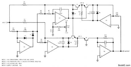
Circuit using National LM118 opamps provides DC output equal to RMS value of sine, triangle, square, or other input waveform with 2% accuracy for 20 V P-P inputs from 50 Hz to 100 kHz. Circuit is usable up to about 500 kHz but with lower accuracy. Direct coupling of input provides true RMS equivalent of combined DC and AC signals. Absolute-value amplifier A1 provides positive input current to A2 and A4 independent of signal polarity. Amplifiers A2-A5 and transistors Q1-Q4 form log multiplier/divider. To calibrate, 10-VDC input signal is applied and R10 is adjusted for 10-VDC output. Transistors should be matched and mounted on common heatsink if possible.-R. C. Dobkin, True RMS Detector, National Semiconductor, Santa Clara, CA, 1973, LB-25.
(View)
View full Circuit Diagram | Comments | Reading(0)
PEAK_TO_PEAK_VOLTMETER
Published:2009/7/15 2:23:00 Author:Jessie
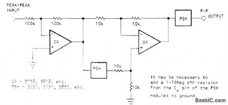
Two Optical Electronics opamps and two peak sense-andhold modules form positive-peak-sense memory that adds negative peak amplitude to entire signal so as to bias negative peak to zero. Input must be restricted to ±5 V full scale (10 V P-P). Output is 0 V for -5 V input and +10 V for +5 V input. Unsymmetrical signals such as +2 V to -8 V still give +10 V output.- Using Peak Sense Memories as Peak-to-Peak Detectors, Optical Electronics, Tucson, AZ, Application Tip 10275. (View)
View full Circuit Diagram | Comments | Reading(839)
METER_OVERLOAD
Published:2009/7/15 2:22:00 Author:Jessie
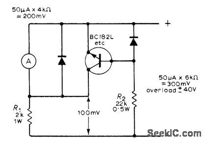
When used with basic meter movement, circuit ensures that overloads merely make pointer run off scale in either direction in controlled manner and press gently against stop pin instead of winding around pin, Values shown will suit most meter movements, but article gives complete design procedure. If voltage being measured is between 350 and 700 mV, use two diodes in series in each position. For voltages between 700 mV and 1 V, use three diodes in series. Diode types are not critical.-C, Shenton, Meter Protection Circuit, Wireless World, Oct. 1972, p 475. (View)
View full Circuit Diagram | Comments | Reading(951)
WIDE_RANGE_VOLTAGE_PROBE
Published:2009/7/15 2:11:00 Author:Jessie
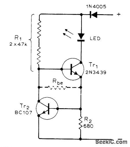
Indicates presence of AC or DC voltages from 3 to 350 V with no ranges witching, using LED as indicator. Transistors serve essentially as constant-current supply for LED Voltage capability can be increased to 450 V by adding suitable base-emitter resistor Rbe; typical value is 60 ohms, which somewhat impairs low-voltage operation.-G. Jones, Voltage Probe, Wireless World, Aug. 1976, p 52.
(View)
View full Circuit Diagram | Comments | Reading(1225)
IC_MODERNIZES_VTVM
Published:2009/7/15 2:10:00 Author:Jessie
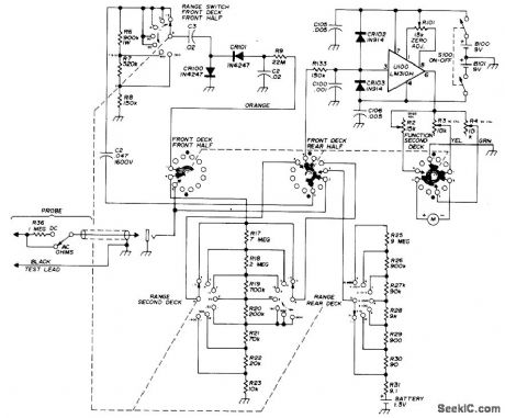
LM310H voltage-follower IC converts VTVM into battery-operated IC voltmeter. Input impedance and scale accuracy are unchanged. Conversion shown is for Heathkit IM-11 VTVM but will apply to most other VTVMs. Semiconductor diodes CR100 and CR101 replace original 6AL5 detector and LM310H high-impedance unity-gain voltage follower replaces original 12AU7. C105 and C106 bypass battery supply and should be connected directly to U100. CR102 and CR103 provide overvoltage protection.-M. Kaufman, How to Convert Your VTVM to an IC Voltmeter, Ham Radio, Dec. 1974, p 42-44. (View)
View full Circuit Diagram | Comments | Reading(2214)
5_min_AC_TIMER
Published:2009/7/14 5:36:00 Author:May

This 555-based circuit will power a load for up to 5 minutes, depending on the setting of R1. Note the transformerless power supply made up of C1, C2, D1, and D2. The timer covers 0 to 5 minutes, or a little more, by measuring the time needed to charge C3 through R1, which is adjustable. To switch the ac power to the load, the timer uses a triac (a solid-state ac switch) instead of a relay. In the power supply, the capacitive reactance of C1 limits the current without generating heat. Use a metal-film capacitor for C1, not an electrolytic. Be sure to observe the voltage rating-use a capacitor rated for at least 200 V (preferably 600 V). Zener diode D1 limits the voltage, and D2 and C2 are the rectifier and filter. (View)
View full Circuit Diagram | Comments | Reading(3528)
VARIABLE_DUTY_CYCLE_TIMER
Published:2009/7/14 5:33:00 Author:May
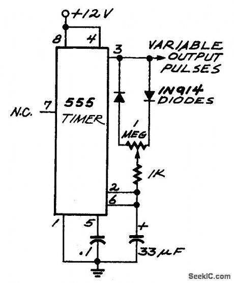
This NE555 circuit produces a variable duty-cycle output. (View)
View full Circuit Diagram | Comments | Reading(0)
AUDIBLE_TIMER
Published:2009/7/14 5:30:00 Author:May
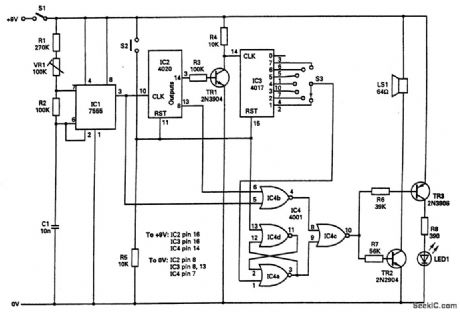
The audible timer relies on the principle of obtaining a relatively long timing period by dividing down the frequency of a high-frequency astable multivibrator. The chip used for the multivibrator is the well-known 555 timer in its CMOS form. The preset resistor VR1 allows the frequency to be set to 273 Hz. This provides the alarm tone. The 273-Hz signal is divided by the 14-stage counter IC2. At pin 8 of the counter, a signal at approximately 1 Hz is used to make the note intermittent. The timing frequency comes from pin 14 of the IC, at which the astable frequency is divided by 214, (16,384), giving a frequency of 1/60 Hz (1 count per minute). The output from pin 14 is inverted by transistor TR1 and fed to the clock input of a second counter (IC3).The outputs of this counter are normally at logical high, except that just one of the outputs is low at each stage of counting. When the counter is reset, output 0 goes high. On the next positive-going clock input, output 0 goes low and output 1 goes high. At each successive high-going clock input, the outputs from 0 to 7 go high, in turn, repeating. The rotary switch (S3) selects the output to be used to indicate the termination of the timing period. The circuit is reset by pressing button S2, which resets both counters and also the flip-flop formed by gates IC4a and IC4d. This turns off the NPN transistor TR2, which drives the loudspeaker, but turns on the PNP transistor (TR3), causing the LED to light.While the RESET button is held, the output from IC2 pin 3 is low, turning off TR1. The counter is incremented every minute until the output selected by S3 goes high. The high level from the selected output sets the flip-flop. The result is a note at 273 Hz, pulsing at the rate of 1 Hz. This is heard from the loudspeaker. The LED flashes on at the same time. Because the mark-space ratio of the astable output is high, the LED is turned on at almost full brightness during the ON periods. (View)
View full Circuit Diagram | Comments | Reading(1981)
LOW_COST_TIMER
Published:2009/7/14 5:16:00 Author:May

Want a simple timer at practically no cost? Depending on what parts you have, you might be able to build this circuit for less than a dollar.
When S1 is closed, C1 begins to charge through R1 toward the 9-V supply. When the voltage at the input of the buffer, pin 3, reaches about 70 percent of the supply voltage, the output switches high for an 0N-time delay function. As long as S1 remains closed, the circuit will maintain the high output at pin 2. Opening S1 resets the timer by allowing C1 to discharge through D1 and R2. (View)
View full Circuit Diagram | Comments | Reading(1307)
CD4050_TIMER
Published:2009/7/14 5:12:00 Author:May
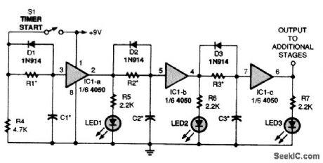
Three stages are used to produce three consecutive time delays. The time delay for each stage is very close to 1.1 RnCn. Diode Dn, allows quicker reset of stage n. (View)
View full Circuit Diagram | Comments | Reading(3606)
CD4528_CMOS_TIMER
Published:2009/7/14 5:24:00 Author:May
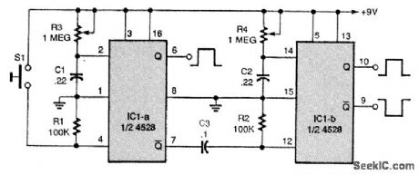
The CMOS timer shown here can easily be cascaded with other similar 4528 circuits. R1C1 and R2C2 determine the timiing. (View)
View full Circuit Diagram | Comments | Reading(4784)
LONG_PERIOD_TIMER
Published:2009/7/14 5:22:00 Author:May
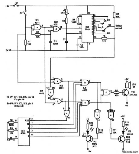
This circuit is based on the 7240 CMOS programmable timer chip (IC3), which has an accuracy of 0.5 percent. It contains a time-base generator, the frequency of which is decided by a resistor and a capacitor. The basic time period is RC seconds; so, given that the maximum value of R is 10 MΩ and the maximum value of C is 1000μF, the maximum time period is 10,000 seconds, (2.8 hours) IC3 also has an eight-stage binary divider chain. The total period available is 27 times the above, which is just over 14 days. In this figure, S1 is an optional power switch. S2 is the switch which is closed to initiate timing. Closing S2 generates a brief low pulse that goes to pin 11 of the timer IC3 and starts the timing. The output of the timer is normally high, but it goes low for the whole of the timing interval. The length of the interval is selected by a rotary switch S3. Pins 1 to 8 of IC3 are the outputs from the eight-stage divider chain. When the counter is reset, they all go high; while timing, they go through an inverted binary sequence. R5 connects the output to the RESET terminal (pin 10), so the counter is reset at the end of the interval. The first stage of the logic consists of two NOR gates and a NAND gate wired as an inverter (part of IC1, 4011). These gates detect the two alarm states. A high output on either pin 8 or pin 9 causes a low output from gate IC2c (pin 10). This makes the RESET input of IC4 low. IC4 is a 14-stage counter with its own oscillator, which begins to oscillate when the RESET is made low. The oscillator has a period of about 25 kHz, which is divided down to produce 1.6 kHz at pin 7 (high-pitched note), 200 Hz at pin 6 (low-pitched note), 6 Hz at pin 1 (fast bleeping), and 1.5 Hz at pin 3 (slow beeping). The remainder of the logic consists of gates producing the fast high-pitched bleep signal, which goes to the red LED (D1) by way of transistor TR2, and the slower, low-pitched bleep, which goes to the green LED (D2) by way of TR3. Both signals go to the speaker LS1 by way of TR1. (View)
View full Circuit Diagram | Comments | Reading(0)
103_COMPATIBLE_MODEM
Published:2009/7/14 4:46:00 Author:May
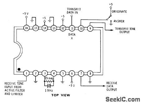
Motorola 4412IC converts serial data, usually to and from uni-versal asynchronous receiver-transmitter, into tones suitable for telephone communication. In originate mode, logic0 is transmitted as 1070 Hz and logic 1 as 1270 Hz. In answer mode, logic 0 is transmitted as 2025 Hz and logic 1 as 2225Hz. Modems are used in pairs, with receiver responding to tone group not being transmitted. Speed capability is up to 300-baud data rate. Output is 300 mVRMS into 100k load.-D. Lan-caster, CMOS Cookbook, Howard W. Sams, Indianapolis, IN, 1977, p 133. (View)
View full Circuit Diagram | Comments | Reading(800)
ABSOLUTE_VALUES_1
Published:2009/7/15 3:38:00 Author:Jessie
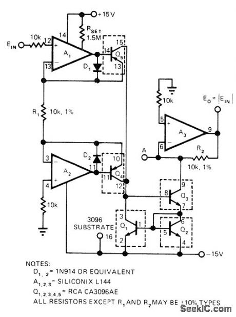
Opamps A1 and A2 act with PNP transistors Q4 and Q5 to form operational rectifier having current-mode output. Current-to-voltage converter A3 uses R2 asscale factor. Input voltage range is determined by common-mode range of opamp and breakdown ratings of components. Circuit shown handles ±10 V signal.-S, Smith, Full-Wave Rectifier Needs Only Two Precision Resistors, EDN Magazine, Jan. 5, 1975, p 56. (View)
View full Circuit Diagram | Comments | Reading(982)
| Pages:29/101 At 202122232425262728293031323334353637383940Under 20 |
Circuit Categories
power supply circuit
Amplifier Circuit
Basic Circuit
LED and Light Circuit
Sensor Circuit
Signal Processing
Electrical Equipment Circuit
Control Circuit
Remote Control Circuit
A/D-D/A Converter Circuit
Audio Circuit
Measuring and Test Circuit
Communication Circuit
Computer-Related Circuit
555 Circuit
Automotive Circuit
Repairing Circuit