
Measuring and Test Circuit
Index 32
LOW_BATTERY_DETECTOR
Published:2009/7/14 2:17:00 Author:May
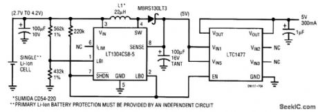
Low-voltage cutoff is desirable in battery-operated systems to prevent deep discharge damage to the battery. The LT1304 micropower boost regulator contains a low-battery detector which is active even when the regulator is shut down. The output of the detector controls both the LTC1477 and the LT1304 5-V boost regulator. In this application, the LTC1477 serves to protect against short circuits (850-mA limit selected) and completely disconnects the load under a low-battery condition. In shutdown, the circuit draws less than 25 μA from the battery. (View)
View full Circuit Diagram | Comments | Reading(0)
AC_POWER_CONTROLLER_FOR_VCR
Published:2009/7/14 2:15:00 Author:May
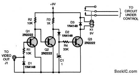
This circuit can be used to switch on a manual-control TV when a VCR signal is present. When the tape starts, video is present at J1 from the VCR video output jack. This is detected, and the dc produced in the detector (D1) circuit turns on Q1, cutting off Q2, and allowing relay driver Q3 to actuate the relay K1. (View)
View full Circuit Diagram | Comments | Reading(1155)
GEIGER_COUNTER_CIRCUIT
Published:2009/7/14 2:13:00 Author:May
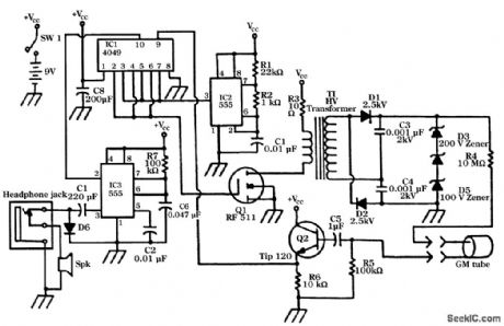
IC2 is a 555 timer set in astable mode. The signal from IC2 is presented to three gates on the 4049 IC1. The 4049 inverts the signal to give an optimum pulse width that switches Q1 on and off. The MOSFET(Q1),in turn,switches the current to a step-up transformer(T1). The stepped-up voltage from T1 first passes through a voltage doubler; the output voltage from this section is approxtmatety 600 to 700 V . Three zener diodes(D3,D4,and D5)are placed across the output of the voltage doubler to regulate the voltage to 500 V. This voltage is connected to the anode on the GM tube through a 10-MΩ resistor. When the GM tube detects a particle,a voltage pulse from the 100-kΩ resistor is amplified and clamped to VCC, Via Q2,an NPN Darlington transistor. The signal from Q2 is inverted by IC1,where it acts as a trigger signal to IC3. IC3 is another 555 timer. The output of IC3 Via pin 3 flashes on LED and provides a click into either the speaker or the headphones . The circuit is powered by a 9-V alkaline battery and draws about 28 mA when not detecting. (View)
View full Circuit Diagram | Comments | Reading(2274)
LOW_BATTERY_MONITOR
Published:2009/7/14 2:12:00 Author:May
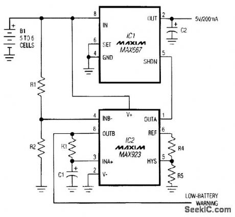
This circuit gives an early warning of declining battery voltage. Then, to allow a controlling processor time for emergency housekeeping chores, such as the storage of register data, the circuit delays system shutdown by a specified time interval (rather than waiting for battery voltage to decline further, to a specified lower level). Circuit components are chosen for low quiescent current, which protects discharged cells by minimizing the battery drain during shutdown: IC1 draws 1 μA, IC2 draws 3 μA, and R1 and R2 draw 3 μA, for a total shutdown current of about 7 μA. R1 and R3=1 MΩ, R2 =280 kΩ, R4=49.9 kΩ, R5=2.4 MΩ, and C1=3.9 μF
(View)
View full Circuit Diagram | Comments | Reading(1211)
1_MC_COUNTER
Published:2009/7/14 2:04:00 Author:May
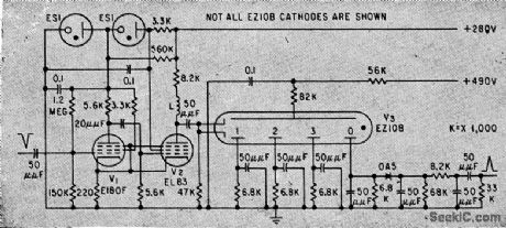
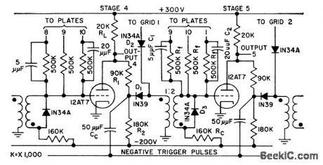
Increasing counting speed to this value requires special hydrogen gas in counter tubes and reduction of tube capacitances. Monostable mvbr V1-V2 is triggered by 5-V negatiye pulses. Cathode resistors of V3 ore bridged by capacitors to reduce effects of capacitive coupling between main and auxiliary cathodes.-K. Apel and P. Berweger, Miniature Gas-Filled Tubes For High-Speed Counting, Electronics, 33:8, p 46-47. (View)
View full Circuit Diagram | Comments | Reading(995)
LOW_POWER_RING_COUNTER
Published:2009/7/14 2:02:00 Author:May
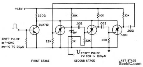
Requires only 6 mw at 1.5V. Reset pulse turns on first stage with its trailing edge.- Transistor Manual, Seventh Edition, General Electric Co, 1964, p 431 (View)
View full Circuit Diagram | Comments | Reading(959)
VARIABLE_TIMING_RING_COUNTER
Published:2009/7/14 2:01:00 Author:May
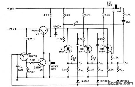
Shift pulses are generated by unijunction transistors, with interval between pulses deter. mined by CT and RT. RT can have different value for each stage of Gaunter, as shown.- Transistor Manual, Seventh Edition, General Electric Co. 1964, p 430. (View)
View full Circuit Diagram | Comments | Reading(935)
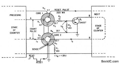
DECIMAL_CODED_COUNTER
Published:2009/7/14 1:59:00 Author:May
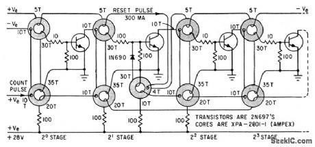
Addition of one core and one diode per decade converts straight-binary counter to decimal-coded counter.-W. R. Johnston, Multiaperture-Core Counters Give Nondestructive Storage Readout, Electronics, 34:24, p 62-64. (View)
View full Circuit Diagram | Comments | Reading(1119)
RING_OF_10_COUNTER
Published:2009/7/14 1:49:00 Author:May
Based on stepping of recognizable sequence of on and off stages along ring at each count pulse, in contrast to conventional ring counters having only one on stage to hold off all other stages.Circuit gives partial diagram, and article gives wiring table for remaining stages. Four on stages are stepped along ring. Time constants of gating circuits limit count rate to 240kc, but components with faster time constants permit operation up to 1 Mc. Ring of 13 is upper limit.-W. Carlson, Ring Counter has Increased Count Capacity, Capacity, Electronics, 31:15, p 89-91. (View)
View full Circuit Diagram | Comments | Reading(907)
SCS_BINARY_COUNTER
Published:2009/7/14 1:48:00 Author:May
Stages are triggered by positive-going edge of input. Silicon con trolled switch is turned on at cathode gate, and turned off at anode gate.- Transistor Manual, Seventh Edition, General Electric Co., 1964, p 429. (View)
View full Circuit Diagram | Comments | Reading(821)
FLASH_BATTERY_TESTER
Published:2009/7/14 1:47:00 Author:May
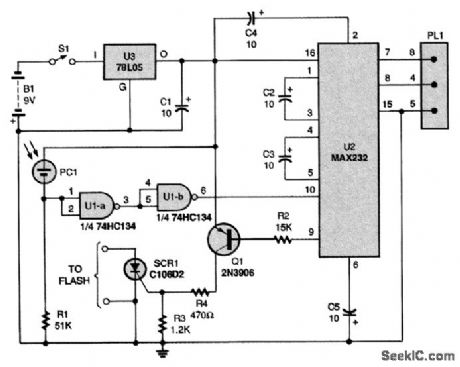
Power from a 9-V battery (B1) is fed to a 78L05 regulator (U3). The IC then produces a regulated 5 V to power the rest of the circuit. A cadmium sulfide photocell, PC1, conducts when a connected flash's ready light comes on and illuminates it. When current flows through PC1, U1-a, and U1-b, two sections of a 74HC134 quad Schmitt trigger NAND gate produce a sharp-edged TTL high. A MAX232, U2, converts the high to an RS233 low that is compatible with the PC's serial port. The MAX232 also takes an incoming serial-port pulse and converts it to TTL levels to fire the flash via SCR1, a C106D2 silicon-controlled rectifier. The circuit works with a BASIC program. That program fires the flash by sending a brief pulse through plug PL1 to the serial port's DTR pin. The program then starts timing how long it takes for the flash to recycle. In other words, the program 'looks at the CTS pin over and over until it sees that it went low. That happens when the photocell is lit by the flash's ready light. The program records the elapsed time and continues counting until 1 minute elapses. At that time, the DTR pin is cycled again to fire the flash, and the process is repeated. The test concludes when the recycle time exceeds 45 seconds. (View)
View full Circuit Diagram | Comments | Reading(1702)
BACKWARD_OR_FORWARD_COUNTER
Published:2009/7/14 1:28:00 Author:May
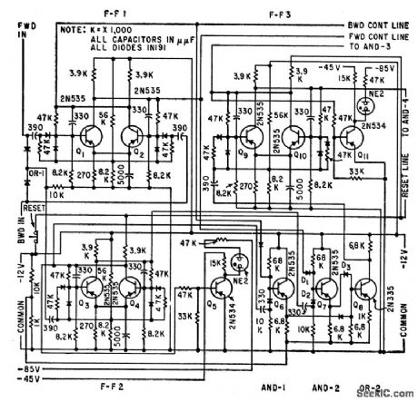
Adds or subtracts pulses under control of appropriate logic circuits. All flip-flops are identical, operating in saturation mode for maximum stability.-H.J.Weber, Binary Circuits Count Backwards or Forwards, Electronics, 32:39, p 82-83. (View)
View full Circuit Diagram | Comments | Reading(784)
TRICOLOR_LED_NiCd_CHECKER
Published:2009/7/14 1:14:00 Author:May
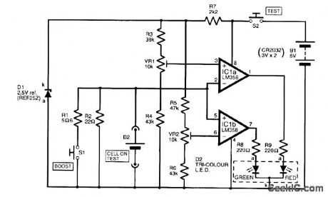
This circuit uses a window comparator and a bicolor LED. VR1 and VR2 set the high and low trip points of the comparators, respectively. The LED shows green for highest voltage (good), yellow for intermediate, and red for low voltage (bad). The circuit can be calibrated for other voltages and is generally useful as a voltage indicator. (View)
View full Circuit Diagram | Comments | Reading(2837)
CABLE_TESTER_TRANSMITTER
Published:2009/7/15 23:28:00 Author:Jessie
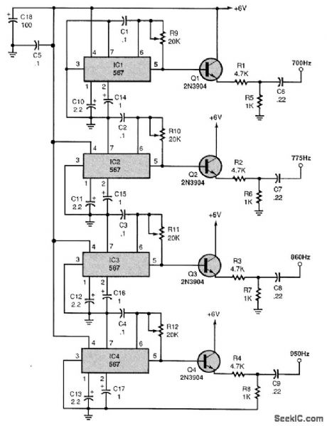
Four 567 tone-decoder ICs, IC1 to IC4, are used to generate four different audio frequencies between 700 and 950 Hz. The capacitor from pin 6 of each 567 to circuit ground, along with the resistor between pins 5 and 6, sets the operating frequency. A 2N3904 NPN transmitter is connected in an emitter-follower circuit to isolate the ICs from output loading. Each output supplies a different audio tone to four wires in a cable. (View)
View full Circuit Diagram | Comments | Reading(2616)
CAPACITIVE_SENSOR_SYSTEM
Published:2009/7/16 1:48:00 Author:Jessie


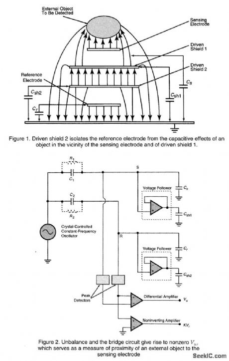
Figure1 illustrates the electric-field configuration of a capacitive proximity sensor of the capaciflector type. This one includes a sensing electrode driven by an alternating voltage, which gives rise to an electric field in the vicinity of the electrode; an object that enters the electric field can be detected by its effect on the capacitance between the sensing electrode and electrical ground. Also, it includes a shielding electrode (in this case, driven shield 1), which is excited via a voltage follower at the same voltage as that applied to the sensing electrode to concentrate more of the electric field outward from the sensing electrode, increasing the sensitivity and range of the sensor. Because the shielding electrode is driven via a voltage follower, it does not present a significant electrical load to the source of the alternating voltage. In this case, the layered electrode structure also includes a reference electrode adjacent to ground, plus a second shielding electrode (driven shield 2), which is ex-cited via a voltage follower at the same voltage as that applied to the reference electrode. Driven shield 2 isolates the reference electrode from the electric field generated by driven shield 1 and the sensing electrode, so a nearby object exerts no capacitive effect on the reference electrode. The excitation is supplied by a crystal-controlled oscillator and applied to the sensing and reference electrodes via a bridge circuit, as shown in Fig. 2. Fixed capacitors C1 and C2 (or, alternatively, fixed resistors R1 and R2) are chosen to balance the bridge-that is, to make the magnitude of the voltage at the sensing-electrode node,S equal the magnitude of the voltage at the reference-electrode node R. The voltages at, S and R are peak-detected and fed to a differential amplifier, which puts out voltage Vu=0. When an object intrudes, it changes Cs, unbalancing the bridge and causing Vu to differ from 0. The closer the object comes to the sensing electrode, the larger |Vu| becomes. An additional output voltage KVr is also available, where K is the amplification factor of a noninverting amplifier and Vr s the voltage on the reference electrode. (View)
View full Circuit Diagram | Comments | Reading(0)
RING_OF_7_COUNTER
Published:2009/7/13 23:48:00 Author:May
Uses surface-barrier transistors in arrangement wherein pattern of four on stages is stepped along ring, per mining maximum number of stages in ring lo be much higher than in conventional rings.-W. Carlson, Ring Counter has Increased Count Capacity, Electronis 31:15, p 89-91. (View)
View full Circuit Diagram | Comments | Reading(1646)
COMMAND_TIME_COUNTER
Published:2009/7/13 23:46:00 Author:May
Used with time-logic matrix to store command times for missile-launching and guidance-control systems.-W.R. Johnston, Multiaperture-Core Counters Give Nondestructive Storage Readout, Electronics, 34:24, p 62-64. (View)
View full Circuit Diagram | Comments | Reading(926)
500_MC_BIQUINARY_COUNTER
Published:2009/7/13 23:39:00 Author:May
Quinary divides input events by 5, using current-mode switches, and binary divides quinary output by 2 to give total division of 10.Chief drawback is difficulty of converting to bcd. All transistors ere 2N2708.-R. Englemann, B-Quinary Scaling: Accuracy and Simplicity at 500 Mc, Electronics, 36:46, p34-36. (View)
View full Circuit Diagram | Comments | Reading(1254)
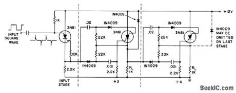
1_MC_COMPLEMENTA_RY_TRANSISTOR_COUNTER
Published:2009/7/13 23:38:00 Author:May
Only one stage draws current from power supply, because on stage has both transistors conducting and off stages have both transistors cut off'. Average power drawn is that of single conducting stage and is independent of number of stages. Circuit prefers off state at startup.-Counter Uses Complementary Transistors, Electronic Circuit Design Handbook, Mactier Pub. Corp., N.Y. 1965, p 129. (View)
View full Circuit Diagram | Comments | Reading(1023)
CAPACITOR_CHECKER
Published:2009/7/16 1:39:00 Author:Jessie
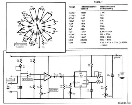
The circuit for the capacitor checker is shown in the figure. Switch S2 is used to select the Mea-sure (M) or Test (T) mode, as required. Assume for the moment that it is in the M position, as shown. Operational amplifier IC1 is configured as a voltage comparator. The values of the resistors have been chosen to provide 86 percent (actually, it is nearer 87 percent) of the supply voltage to the noninverting input, pin 3. Meanwhile, the capacitor being measured, Ct, charges through resistor R1, so the voltage across it rises and follows the form shown in Fig. 2.R1 is selected from a chain of resistors using the rotary range switch, S1 (inset). The value of R1 in the chain will be such that with a capacitor at the top of the range selected (e.g.a100-nF capacitor on the 100-nF range), the time constant will be 1.66 s. The values of R1, required to provide this time constant on the various ranges are shown in Table 1. Assuming that the test capacitor Ct is discharged to begin with, after two time constants have elapsed, the voltage across the capacitor will rise above 86 percent of the supply. The op amp switches off, with pin 6 becoming low. While IC1 pin 6 is high (during the initial stages of C, charging), IC2 pin 4 is maintained in a high state, which enables the IC. When the capacitor charges through two time constants, IC1 pin 6 becomes low, IC2 is disabled, and the flashing stops. The nominally low state of IC1 output would still be high enough to enable IC2 if connected directly, and the two diodes (D1 and D2) correct this. Resistor R6 maintains IC2 pin 4 low in the absence of a high state from IC1 output. The rate at which pulses are produced depends on the values of fixed resistors R8 and R9 and preset potentiometer VR2, in conjunction with capacitor C2. With the values chosen, they will be delivered at between 1 and 10 per second approximately, depending on the adjustment of VR2. VR2 will be adjusted so that exactly three flashes per second are provided. Ten flashes, therefore, correspond to 3.33 s, which is equal to two time constants for a capacitor at the limit of the range selected. (View)
View full Circuit Diagram | Comments | Reading(2021)
| Pages:32/101 At 202122232425262728293031323334353637383940Under 20 |
Circuit Categories
power supply circuit
Amplifier Circuit
Basic Circuit
LED and Light Circuit
Sensor Circuit
Signal Processing
Electrical Equipment Circuit
Control Circuit
Remote Control Circuit
A/D-D/A Converter Circuit
Audio Circuit
Measuring and Test Circuit
Communication Circuit
Computer-Related Circuit
555 Circuit
Automotive Circuit
Repairing Circuit