
power supply circuit
Index 78
PULSE_HEIGHT_DETECTOR
Published:2009/7/16 5:31:00 Author:Jessie
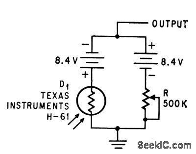
Photodiode held against screen of scope unbalances bridge when illuminated by pulse on screen. Bridge output can control another scope for displaying and measuring pulses whose amplitude and period vary randomly.-I. Baird, Pulse Frequency Measured by Photoconductor and Scopes, Electronics, 38:13, p 77. (View)
View full Circuit Diagram | Comments | Reading(1021)
SIGNAL_POWERED_TRANSPONDER
Published:2009/7/16 5:30:00 Author:Jessie
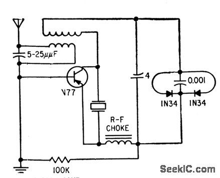
Power received at frequency of tuned antenna circuit energizes crystal transistor stage, to make it oscillate at a different frequency. Can be used in aircraft or vehicle to make it radiate position-determining signal when interrogated by powerful transmitter at base station. –L. R. Crump, Radio Waves Power Transistor Circuits, Electronics, 31:19, p 63-65. (View)
View full Circuit Diagram | Comments | Reading(1247)
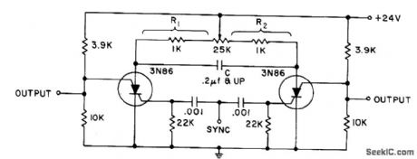
GATED_DIODE_BEACON_MODULATOR
Published:2009/7/16 5:30:00 Author:Jessie

Replaces hydrogen-thyratron line-pulsing modulators formerly used to plate-pulse pencil triode in beacon transmitter. Maximum pulse rate is 5,000 pps. -W. H. Lob, Solid-State Pulse Modulator, Electronics, 33:30, p 72-74. (View)
View full Circuit Diagram | Comments | Reading(833)
SCS_SQUARE_WAVE_GENERATOR
Published:2009/7/16 5:30:00 Author:Jessie
R1-C determines half the period, and R2-C the remainder. R1 should equal R2 for square wave output. Potenliometer varies pulse width without affecting frequency. Outputs are equal and oppositely phased.- Transistor Manual, Seventh Edition, General Electric Co., 1964, p 434. (View)
View full Circuit Diagram | Comments | Reading(752)
CRASH_RESISTANT_BEACON
Published:2009/7/16 5:29:00 Author:Jessie
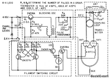
Designed to withstand shocks up to 1,100 g and extreme environments, 5.7-1b beacon is thrown free of crashing aircraft and automatically starts transmitting pulse-modulated 243-Mc distress signal. -D. M. Makow, Radio Beacon Helps Locate Aircraft Crashes, Electronics, 33;4, p 54-56. (View)
View full Circuit Diagram | Comments | Reading(848)
LINEAR_TECHNOLOGY_POWER_SOLUTIONS
Published:2009/7/13 2:49:00 Author:May
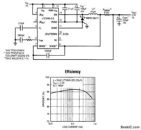
An increasing number of portable devices need 5-V-to-3.3-V converters. High efficiency at up to 1 A is needed to power 3.3-V ICs, such as power-hungry high-speed microprocessors. The LTC1265-3.3 high-efficiency switching regulator circuit shown generates up to 1 A at 3.3 V. The LTC1265-3.3 utilizes a constant OFF-time current-mode architecture for excellent line and load regulation and contains an internal P-channel power MOSFET with 0.3 Ω ON resistance, as well as a low-battery detector. The output current is user-programmable by selection of the current sense resistor Rsense according to the formula Iout = 100 mV /Rsense. Short-circuit protection is inherent in the current-iiiode architecture and limits the maximum current. The LTC1265 draws only 160 μA quiescent current under no load and just 5 μA when placed in shutdown. (View)
View full Circuit Diagram | Comments | Reading(963)
RF_PREAMP_SUPPLY
Published:2009/7/13 2:49:00 Author:May
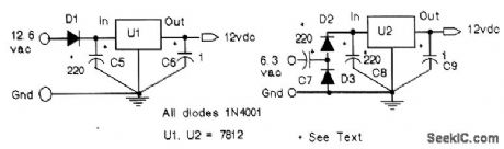
Early tube-type receivers used filament voltages of 6.3 and 12.6 Vac, but had no low-voltage dc power supplies. The figures show how to borrow a little of the filament voltage, which is rectified and regulated to provide 12 Vdc for the preamp. In the 6.3-Vac version, diodes D2 and D3 act as a simple voltage doubler to step the input voltage up to approximately 15 Vdc. While the 220-μF capacitors used for the voltage doubler are sufficient for the load presented by the preamp, they will not provide the 115 V dc to the input of the regulator at more than about a 25-mA load. If other circuits will be used with these dc power sources, then the 220-μF capacitors should be increased ac-cordingly (2200 μF will provide about 65 mA regulated output). (View)
View full Circuit Diagram | Comments | Reading(904)
N100-multifunctional power control integrated circuit
Published:2011/7/27 10:17:00 Author:Nancy | Keyword: multifunctional power control
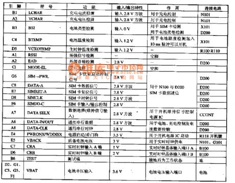
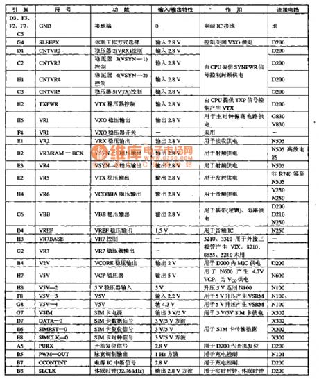
The N100 is a multifunctional power control integrated circuit widely used in the Nokia mobile phones.
Functions and features:The N100 integrated circuit includes sleep work mode option, various voltage stabilizer circuits, pulse width modulation circuit, RF power supply control circuit, the battery type detection circuit, temperature detection circuit batteries, SIM card powered start, data, reset, clock, input/output control circuit, the universal serial data and clock, the main clock temperature testing, charging current and voltage detection circuit, and some other auxiliary function circuits.
(View)
View full Circuit Diagram | Comments | Reading(1581)
TWO_TRIODE_CASCODE_MULTIVIBRATOR
Published:2009/7/16 5:01:00 Author:Jessie
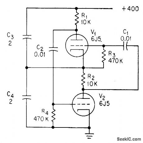
Two capacitors in voltage-divider storage circuit control dual-triode multivibrator to produce linear sawtooth waveform, square wave,sine wave, or pulse.-C. Sing, Advantages of Free-Running Cascode Multivibrators,Electronics, 37:5, p 28-29. (View)
View full Circuit Diagram | Comments | Reading(781)
MAGNETICALLY_COUPLED_MVBR
Published:2009/7/16 5:00:00 Author:Jessie
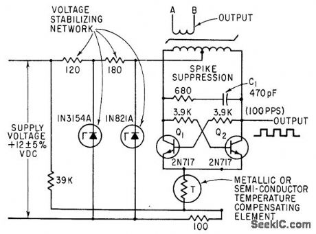
Nonlinear element T in common-emitter lead stabilizes against temperature variation to within 0.1% over 150℃ range. Output is 100 pps. –M. Ingenito, Magnetically Coupled Multivibrators, Electronics, 36:13, p 42-43. (View)
View full Circuit Diagram | Comments | Reading(685)
EPIIAXIAL_NOR_GATE
Published:2009/7/16 4:59:00 Author:Jessie
Operates at up to 8Mc from -55°C to+150°C.-D,Hall Using Epitaxial Transistors in Switching and R-F Circuits. Electronics, 34:13, p 52-53. (View)
View full Circuit Diagram | Comments | Reading(733)
MONOSTABLE_PULSE_FORMER
Published:2009/7/16 4:58:00 Author:Jessie
Output stage of driver serves also as first stage of monostable multivibrator, with saving in components. Here Q2 is output of Schmitt trigger and first stage of monostable mvbr Q2-Q1. –R. L. Paul and A. S. Ottenstein, Eliminating the First State of a Monostable Multivibrator, Electronics, 35:36, p 54-55. (View)
View full Circuit Diagram | Comments | Reading(915)
RESISTOR_TRANSISTOR_NOR_GATE
Published:2009/7/16 4:58:00 Author:Jessie
Circuit is basic building block of binary full adder for high speed encoding Transistor is 2N1499.-S. C. Chao, High Speed Encoding with Resistor-Transistor-Logic Circuits, Electronics, 35-6.p 48-51. (View)
View full Circuit Diagram | Comments | Reading(810)
SINGLE_TRANSISTOR__ONE_SHOT
Published:2009/7/16 4:57:00 Author:Jessie
Requires fewer components and gives higher reliability. –T. F. One-Transistor Single-Shot, Electronics, 34:16, p 66. (View)
View full Circuit Diagram | Comments | Reading(1298)
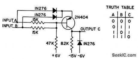
NEON_WITH_PNP_EXCLUSIVE_OR_LOGIC
Published:2009/7/16 4:57:00 Author:Jessie
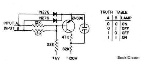
Neon lamp glows when inputs are in agreement. Indicator will follow only one control level if other input is at fixed voltage such as logic 0; lamp will then turn off whenever control input is at logic 1. Similarly, if fixed voltage is logic 1, lamp will turn off when control input is at logic 0.-Exclusive OR Uses One Transistor, Electronic Circuit Design Handbook, Mactier Pub. Corp., N.Y., 1965, p 213. (View)
View full Circuit Diagram | Comments | Reading(773)
DELAYED_OUTPUT_PULSE
Published:2009/7/16 4:56:00 Author:Jessie
Only three transistors are required to generate output rectangular pulse that is delayed a predetermined time after arrival of input pulse. Delay time is determined by C1, R3, and R4, and is about 10 microsec for values shown. Output pulse width is also about 10 microsec. -T. R. Ferrara, Delayed Pulse Generator, EEE, 13:10, p 71 (View)
View full Circuit Diagram | Comments | Reading(729)
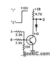
NPN_AND_GATE
Published:2009/7/16 4:55:00 Author:Jessie
Two diodes act as conventional and gate with transistor and its collector supply, using few components. Intended for 0 and -6 V logic.-Exclusive OR Uses One Transistor, Electronic Circuit Design Handbook, Mactier Pub. Corp., N.Y., 1965, p 213. (View)
View full Circuit Diagram | Comments | Reading(900)
CALIBRATED_MILLIMICROSECOND_PULSER
Published:2009/7/16 4:55:00 Author:Jessie
Uses coaxial discharge line to produce precise short pulses on keyed single-shot basis or of constant repetition rate. Works into 50-ohm load.-E. J. Martin, Jr., Calibrated Source of Millimicro second Pulses, Electronics, 32:16, p 56-57. (View)
View full Circuit Diagram | Comments | Reading(751)
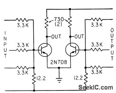
DOUBLE_NOR_GATE
Published:2009/7/16 4:55:00 Author:Jessie


Pulse repetition rate is 1Mc, fanin is 3, and fanout is up to 6, with 30-mw dissipation for 7-v supply.-Double NOR Gate for Dense Packaging, Electronics, 36:12, p 100. (View)
View full Circuit Diagram | Comments | Reading(834)
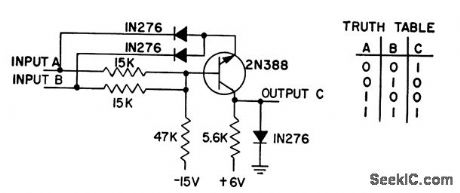
PNP_EXCLUSIVE_OR_LOGIC
Published:2009/7/16 4:54:00 Author:Jessie
For use with0 (ground) and -6 v logic system. Can be adapted readily to most other logic levels. Produces logic 1 when inputs disagree.-Exclusive OR Uses One Transistor, Electronic Circuit Design Handbook, Mactier Pub. corp,N.Y.1965,p213. (View)
View full Circuit Diagram | Comments | Reading(842)
| Pages:78/291 At 206162636465666768697071727374757677787980Under 20 |
Circuit Categories
power supply circuit
Amplifier Circuit
Basic Circuit
LED and Light Circuit
Sensor Circuit
Signal Processing
Electrical Equipment Circuit
Control Circuit
Remote Control Circuit
A/D-D/A Converter Circuit
Audio Circuit
Measuring and Test Circuit
Communication Circuit
Computer-Related Circuit
555 Circuit
Automotive Circuit
Repairing Circuit