
power supply circuit
Index 71
POLARITY_INDICATOR
Published:2009/7/15 20:25:00 Author:Jessie
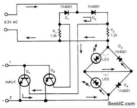
Q1 and Q2 at input should be Darlington transistors to minimize loading on input signal. With no input, current flows through R1D1 and R2D2 networks on alternate half-cycles, Positive signal at input 1 turns on Q1, shunting sum of current through D3 and lighting positive-indicating LED in diode bridge. Similarly, negative voltage on 1 turns on other LED. Supply requirement of 6.3 VAC can usually be obtained from digital multimeter with which indicator is used.-R. A. Snyder, Simple Polarity Indicator Suits DMM's or DPM's, EDN Magazine, Nov. 5, 1977, p 110. (View)
View full Circuit Diagram | Comments | Reading(1977)
ELECTROSCOPE
Published:2009/7/15 20:15:00 Author:Jessie
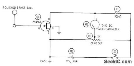
Gate of FET floats, being connected only to smooth metal rod tipped with polished brass ball. Rod is insulated from housing with polystyrene washer in large hole. Static drain current of FET is balanced out of meter with R2 when ball is clear of operator's body or other object. Meter deflection then is proportional to intensity of charge on body brought near ball and on separation. Electroscope will respond to vigorously stroked paper or just-used comb.-R. P. Turner, FET Circuits, Howard W. Sams, Indianapolis, IN, 1977, 2nd Ed., p 153-154. (View)
View full Circuit Diagram | Comments | Reading(5056)
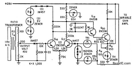
SUBSCRIBER_LINE_INTERFACE_CIRCUIT_POWER_SUPPLY
Published:2009/7/14 3:15:00 Author:May
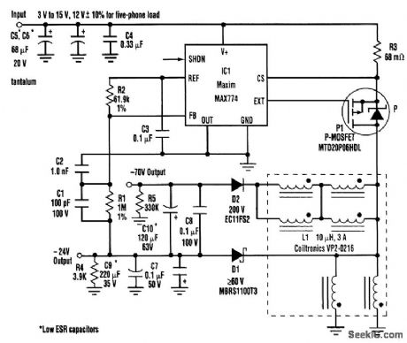
A new multiwinding transformer (configurable by the user for a variety of applications) enables an inverting controller to produce the high negative voltages required by an ISDN board or other telephone line card. Such line cards use a subscriber-line interface circuit (SLIC), such as the 79R79 ringing SLIC from AMD. This IC generates the off-hook and on-hook signal transmission, ring-tone generation, and ring-tip detection that constitute an analog telephone interface. For off-hook signal transmission, it requires a tightly regulated -24 or -48 V; to generate ring tones, it requires a loosely regulated -70 V. The five -ringer-equivalent requirement demands 9 to 10 W from the -70-V output, which translates to a full-load lout of about 150 mA. IC1 is an inverting switching regulator that usually converts a 3- to 16-V input to a fixed output of -5 V or an adjustable output. In the circuit shown, three pairs of windings in series (provided by a single off-the-shelf multiwinding transformer) enable IC1 to generate the high voltages needed by a SLIC IC1 (D1). Connecting a diode and output capacitors (C7 and C9) at the first or second pair of windings produces -24 V (as shown) or -48 V, respectively. Feedback to the IC via R1 and R2 achieves tight regulation at this output. The trans-former turns ratios establish a loose regulation at the -70-V output. The circuit can service a five telephone load (10 W) from an input of 12 V, ±10 percent. It operates down to 3 V and produces about 2.4 W at 3.3 V and 3.9 W at 5 V. The -70-V output depends on cross-regulation with respect to the -24-V output. It is, therefore, affected by relative loading on the two outputs (i.e., whether one is heavily loaded and the other lightly loaded, or vice versa). (View)
View full Circuit Diagram | Comments | Reading(1401)
11X_PULSE_STRETCHER
Published:2009/7/15 5:33:00 Author:Jessie
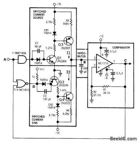
Provides negative output pulse width equal to positive input pulse multiplied by 1 + R4/R3, which is 11 for values shown. Output pulses are TTL-or DTL-compatible. Minimum output pulse width is 70 ns, and maximum is 1/11 of pulse repetition rate. Circuit consists of switched current source, switched current sink, integrating capacitor, and comparator. Q1 and Q2 act as switches for current sources Q3 and Q4, while C1 and C2 reduce turn-on and turnoff times of switches. CR1 and CR2 provide temperature compensation for Q3 and Q4. AND gate compensates for propagation delay in NOR gate, to ensure that current sink is switched on by trailing edge of input pulse. Add inverter if output must be same polarity as input.-F. Tarico, Linear Circuit Multiplies Pulse Width, EDN|EEE Magazine, Dec. 1, 1971, p 45-46. (View)
View full Circuit Diagram | Comments | Reading(860)
PHASE_INVERTER_FOR_CODE_CONVERTER
Published:2009/7/15 5:29:00 Author:Jessie
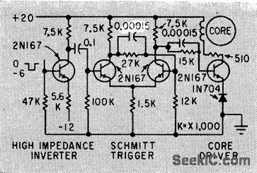
In addition to phase reversal of input signal, single npn transistor provides isolation between negative input pulse and core driver, which is Schmitt trigger having discrimimation level within 10% of -4.5 v including phase inverters. Signals below that level are disregarded. Signal range from 6 to 12 v will cause pulse output from Schmitt, with duration dependent on duration of input signal. When Schmitt trigger emits pulse, 1N704 driver supplies 30-ma current pulse, writing a ONE into ifs associated core.-R. Wasserman und W. Nutting, Solid-Stale Digital Code-to-Code Converter, Electronics,32:50, p 60-63. (View)
View full Circuit Diagram | Comments | Reading(879)
PREFERRED_PRF_GENERATOR
Published:2009/7/15 5:26:00 Author:Jessie
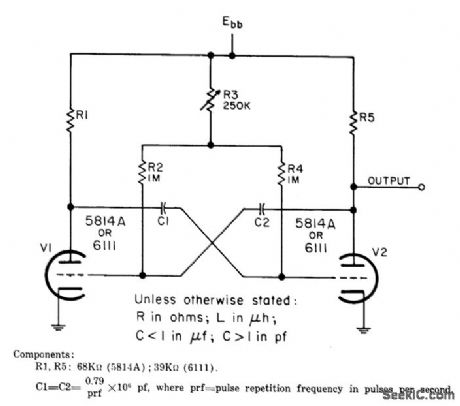
Astable plate-to-grid coupled mvbr serves as moderately stable repetition-rate generator having greater frequency stability than blocking oscillator and fewer components than Wien-bridge oscillator. One drawback is that output impedance for positive pulses equals plate load resistance, which must be relatively high for good frequency stability. Output is 260 V for 5814A and 125 V for 6111. Maximum prf is 8,000 pps.-NBS, Handbook Preferred Circuits Navy Aeronautical Electronic Equipment, Vol. I, Electron Tube Circuits, 1963, PC 40, p 40-2. (View)
View full Circuit Diagram | Comments | Reading(751)
INVERTER_REFERENCE_ELEMENT
Published:2009/7/15 5:23:00 Author:Jessie
Accuracy and stability of d-c to 400-cps a-c inverter are achieved by temperature compensation of IN2169A zener reference element. Silicon transistors are used where d-c levels are handled.-R. Wileman, linear Circuits Regulale Solid-Stale Inverler, Electronics, 33:16, p 61-63. (View)
View full Circuit Diagram | Comments | Reading(785)
INVERTER_BASE_SPEED_UP_WINDINGS
Published:2009/7/15 5:20:00 Author:Jessie
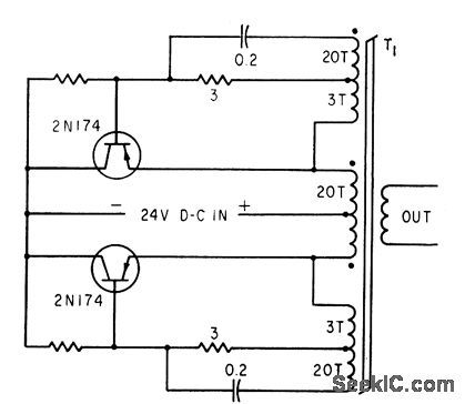
Individual speed-up windings and series capacitors for each transistor base reduce switching times to as little as 4 microsec for 2N174's and to 2 microsec for some germanium power transistors.-A. G. Lloyd, Speed-up Circuits Improve Switching of Transistor Inverters, Electronics, 34:45, p 92-94. (View)
View full Circuit Diagram | Comments | Reading(1145)
D_C_AMPLIFIER_SERVES_AS_VOLTAGE_REGULATOR
Published:2009/7/15 5:19:00 Author:Jessie
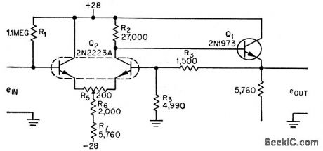
Output voltage of series pass transistor Q1 is compared to input voltage serving as reference voltage by differential amp liner Q2 and variations are fed back to reduce difference. Feedback ratio of 0.67 gives overall gain of 1.3 and 10-ohm output impedance.-W. S. Zukowsky, Aligning Saturn Missile's Guidance System, Electronics, 37:8, p 26-27. (View)
View full Circuit Diagram | Comments | Reading(866)
96_MILLISEC_PULSE_STRETCHER
Published:2009/7/15 5:10:00 Author:Jessie
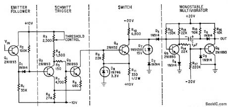
Monostable multivibrator stays on for 96 millisec after Schmitt trigger goes off, while C discharges through R12. -J. R. Giroux, Multi's Output Duration Controlled by Input, Electronics, 38:4, p 88-89. (View)
View full Circuit Diagram | Comments | Reading(913)
0_100000_V_IN_100_μV_STEPS
Published:2009/7/15 21:01:00 Author:Jessie
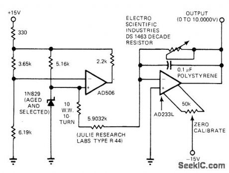
Constant cur-rent from AD506 opamp drives zener, with 5.16K resistor providing optimum current through zener for temperature-drift cancellation. Chopper-stabilized opamp scales output of zener over full range, Offset-voltage pot serves for zero calibration. Reference voltage is stable to about 11 PPM per year.4. Williams, Don't Bypass the Voltage Reference That Best Suits Your Needs, EDN Magazine, 0ct. 5, 1977, p 53-57. (View)
View full Circuit Diagram | Comments | Reading(1060)
_5__15_AND__25_V
Published:2009/7/15 21:00:00 Author:Jessie
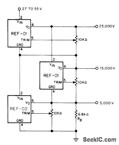
Stacking of Precision Monolithics REF-02 5-V reference with two REF-01 10-V references gives outputs increasing in steps of 10.000 V from 5,000 V. Any number of additional references can be stacked in same way up to line-voltage limit of 130 V for references, provided total load current does not exceed about 21 mA. Input change from 21 to 55 V produces output change less than noise volt-age of devices in circuit shown.- +5 V Precision Voltage Reference/Thermometer, Precision Monolithics, Santa Clara, CA, 1978, REF-02, p7. (View)
View full Circuit Diagram | Comments | Reading(835)
BAND_GAP_PRECISION_REFERENCE
Published:2009/7/15 20:58:00 Author:Jessie
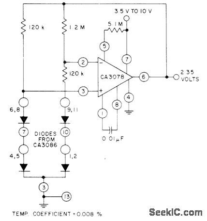
Uses diodes from CA3086 array and CA3078 micro-power opamp to develop 2.35-V precisely controlled output reference that is almost indepen-dent of temperature. –″Circuit Ideas for RCA Linear ICs,″RCA Solid State Division, Somerville, NJ, 1977, p 18. (View)
View full Circuit Diagram | Comments | Reading(1023)
120_kHz_TO_4_MHz
Published:2009/7/15 21:17:00 Author:Jessie
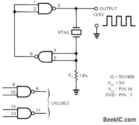
Square-wave output of about 3.5 V can be obtained with SN7400 quad NAND gate, quartz crystal of desired frequency, and single resistor. One of unused gates may be used to gate generator output. Insertion of crystal in socket shocks crystal into oscillation at its resonant frequency, for generating square-wave output over most of frequency range. Waveform approaches clipped sine wave near 4 MHz. Output is suitable for triggering SN7490 decade counters reliably, with normal fan-out.-E. G. Olson, 2 Gates Make Quartz Oscillator, EDN Magazine, May 5, 1973, p 74. (View)
View full Circuit Diagram | Comments | Reading(1330)
ANALOG_TYPE_RATIO_COMPUTER
Published:2009/7/15 21:16:00 Author:Jessie
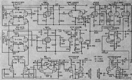
Computes and automatically displays on oscilloscope the ratio of two time-varying quantities, such as noise suppression factor of tube shot noise. Five main parts are sampler, shaper of ramp or step in each channel, amplitude comparator, converter for final indicator, and timing unit that provides sampling signal-J. Tamiya, Automatic Display of Noise Suppression Factor, Electronics, 33:6, p 55-57. (View)
View full Circuit Diagram | Comments | Reading(851)
SQUARE_WAVE_GENERATOR
Published:2009/7/15 21:15:00 Author:Jessie
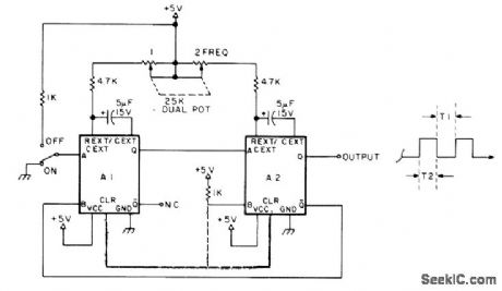
Uses two 74122 retriggerable mono MVBRs with clear. Two single pots may be used in place of dual 25K pot if up and down times of output must be independently adjustable.-B. Voight, The TTL One Shot, 73 Magazine, Feb. 1977, p 56-58. (View)
View full Circuit Diagram | Comments | Reading(4499)
10_V_MICROPOWER
Published:2009/7/15 21:13:00 Author:Jessie
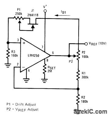
Low-drift voltage reference has standby current less than 100 μA, using LM4250 opamp to convert zero-temperature-coefficient current to desired reference voltage output. Adjust Pl for low output tem-perature coefficient, and adjust P2 for exact reference desired.- Linear Applications, Vol. 2, National Semiconductor, Santa Clara, CA, 1976, LB-34. (View)
View full Circuit Diagram | Comments | Reading(890)
10_V_USING_STANDARD_CELL
Published:2009/7/15 21:12:00 Author:Jessie
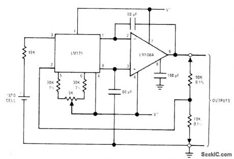
Low drift and low input current of National LM121 differential amplifier provide buffering for standard cell with high accuracy. Typical long-term drift for LM121 operating at constant temperature is less than 2 μV per 1000 h. Circuit should be shielded from air currents. When power is not applied, disconnect standard cell to prevent it from discharging through internal protection diodes.- Linear Applications,Vol, 2, National Semiconductor, Santa Clara, CA, 1976, AN-79, p8. (View)
View full Circuit Diagram | Comments | Reading(986)
__15_V_AT_100_mA
Published:2009/7/15 21:11:00 Author:Jessie
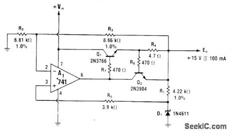
Boost transistor Q1 is added inside feedback loop to amplify output current of A1 to 100 mA at scale-up reference of + 15 V from 6, 6-V value of zener. R4 and Q2 provide protection against load shorts.-W. G. Jung, IC Op-Amp Cookbook, Howard W. Sams, Indianapolis, IN, 1974, p 152-155. (View)
View full Circuit Diagram | Comments | Reading(843)
5_V_AT_75_mA
Published:2009/7/15 21:09:00 Author:Jessie
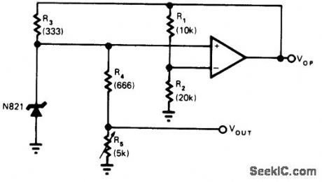
Circuit uses single pot with standard opamp to ad just output voltage and simultaneously set current of 6.2-V zener at optimum value for temperature stability. With some opamps, emitter-follower may be needed at opamp output to supply necessary zener current. Technique eliminates need for separate zener current adjustment or permits use of lower-cost zener.-K. Hanna, Single Control Adjusts Voltage Reference, EDN Magazine, June 5, 1976, p 117. (View)
View full Circuit Diagram | Comments | Reading(899)
| Pages:71/291 At 206162636465666768697071727374757677787980Under 20 |
Circuit Categories
power supply circuit
Amplifier Circuit
Basic Circuit
LED and Light Circuit
Sensor Circuit
Signal Processing
Electrical Equipment Circuit
Control Circuit
Remote Control Circuit
A/D-D/A Converter Circuit
Audio Circuit
Measuring and Test Circuit
Communication Circuit
Computer-Related Circuit
555 Circuit
Automotive Circuit
Repairing Circuit