
power supply circuit
Index 74
PRF_GENERATOR_1
Published:2009/7/15 23:18:00 Author:Jessie
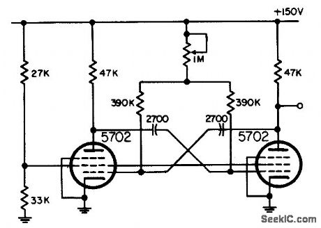
Used as repetition rate generator in airborne radar. Gives greater frequency stability than blocking oscillator and greater economy of components than Wien-bridge oscillator.-NBS, Handbook Preferred Circuits Navy Aeronautical Electronic Equipment, Vol. 1, Electron Tube Circuits, 1963, p N5-1. (View)
View full Circuit Diagram | Comments | Reading(1051)
RELAY_ONLY_MVBR
Published:2009/7/15 23:16:00 Author:Jessie
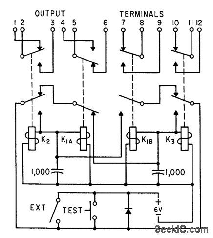
Consumes power only during switching. Can provide bistable, monostable, or astable operation at frequencies from a few operations per second to a few operations per hour.-R. L. Ives, Multivibrator for Low Frequencies Uses Relays, Electronics, 34:32, p 166-169. (View)
View full Circuit Diagram | Comments | Reading(818)
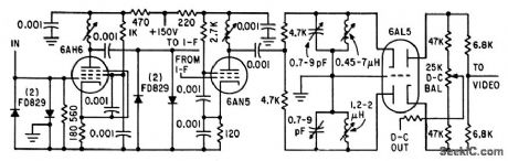
80_DB_DYNAMIC_RANGE_AT_8_MC
Published:2009/7/15 23:16:00 Author:Jessie
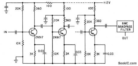
Uses five identical cascaded stages with filter to re store sinusoidal waveform. Phase-shill variations are only 10. Limits input signal by collector current cutoff only. Used in multichannel-tracking receiving system.-S. P. VV.Stranddorf, High-Frequency limiter Amplifier Solves Phase-Shift Problems, Electronics, 35:46, p 44-45. (View)
View full Circuit Diagram | Comments | Reading(752)
LINEAR_VOLTAGE_FREQUENCY_CONVERTER
Published:2009/7/15 23:16:00 Author:Jessie
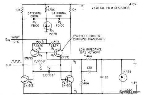
Addilion of two transistors to conventional astable mvbr gives constant-current charging of cross-coupling capacitors C1 and C2. Output frequency then varies linearly from 2,000 to 7,000 cps as d-c input rises from 0 to 5 V.-R. W. Biddlecomb, Latest Multivibrator Improvement: Linear Voltage-to-Frequency Converter, Electronics, 36:17, p 64-65. (View)
View full Circuit Diagram | Comments | Reading(819)
DIODE_PAIRS
Published:2009/7/15 23:15:00 Author:Jessie
High-speed silicon diode pairs in two-stage limiter for telemetry, measuring, aft systems, and f-m systems give 5% linearity over 6-Mc bandwidth. Associated discriminator uses two single poles resistively coupled to driving tube.-High-Speed Diodes Make Limiting Smooth, Electronics, 35:27, p80. (View)
View full Circuit Diagram | Comments | Reading(924)
_10_V_WITH_BOOTSTRAPPED_OPAMP
Published:2009/7/15 22:24:00 Author:Jessie
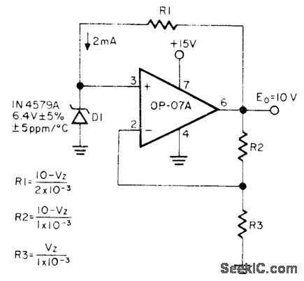
High-stability Precision Monolithics 0P-07A bipolar-input opamp with ultralow offset voltage provides precise 10 V virtually independent of changes in supply voltage, ambient temperature, and output loading. Choose value of R1 to maintain zener current at exactly 2 mA, using 5 PPM/'C resistor. All resistor values are determined from exact zener voltage Vz, as given by equations alongside circuit.-D. Soderquist and G. Erdi, The OP-07 Ultra-Low Offset Volt-age 0p Amp-a Bipolar Op Amp That Challenges Choppers, Eliminates Nulling, Precision Monolithics, Santa Clara, CA, 1975, AN-13, p 8 (View)
View full Circuit Diagram | Comments | Reading(905)
UPWARD_SCALING
Published:2009/7/15 22:23:00 Author:Jessie
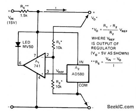
Output of AD580 threeterminal voltage regulator is multiplied in shunt regulator loop using opamp A,. Resulting reference voltage VEEF is scaled upward by reciprocal of feedback divider R1/R2. Resulting reference is immune to input variations. Reference output range is from 5 V up to voltage limit of opamp used. If desired, reference value can be programmed via R1. LED lights to show proper operation of circuit.-W. G. Jung, Programmable Voltage Reference is Stable, yet Simple, EDN Magazine, Nov. 5, 1975, p 98 and 100. (View)
View full Circuit Diagram | Comments | Reading(1078)
+82_V
Published:2009/7/15 22:22:00 Author:Jessie
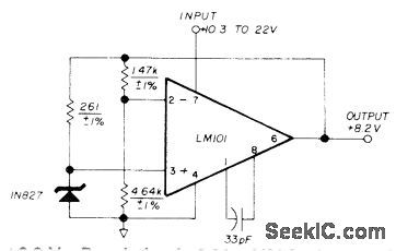
Regulation is 0.01 mV/V for inputs of 10.3-22 V, and temperature stability is ±0.05% from -55℃ to 125℃. Short-circuit protection for reference is provided intemally. Uses National LM101, LM301A, or equivalent opamp.-D. W. Nelson, Introduction to Operational Amplifiers, Ham Radio, March 1978, p 48-60. (View)
View full Circuit Diagram | Comments | Reading(923)
WIDE_INPUT_VOLTAGE_RANGE
Published:2009/7/15 22:21:00 Author:Jessie
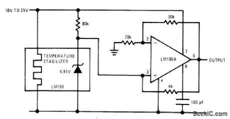
Power for LM199 temperature-stabilized voltage reference is obtained from output of LM108A buffer opamp, to permit use with to -25 V supply. 80K resistor is used in unregulated input to make circuit start properiy when power is applied.- Linear Applications, Vol. 2, National Semiconductor, Santa Clara, CA, 1976, AN-161, p 6. (View)
View full Circuit Diagram | Comments | Reading(1069)
INPUT_ATTENUATOR
Published:2009/7/16 1:50:00 Author:Jessie
Low-distortion automatic input attenuator for modern communication receiver is activated at input signal levels above 100 μV. For range of 1-30 MHz, use PIN diodes such as HP5082-3081, Intermodulation distortion products of attenuator are about 85 dB down for two 1-V signals.-U. L. Rohde, 0ptimum Design for High-Frequency Communications Receivers, Ham Radio, Oct. 1976, p 10-25.
(View)
View full Circuit Diagram | Comments | Reading(1295)
1_mA_CURRENT_SINK
Published:2009/7/16 1:48:00 Author:Jessie

A ftxed current flows through any load that is connected between the positive supply and Q1's collector. The noninverting terminal of the op amp is grounded, and negative feedback flows between the output of the circuit (Q1's emitter) and the inverting terminal. The voltage across R1 is thus equal to the voltage at the inverting terminal (approximately 0.55 V), so a fixed current of about 1 mA flows through the load, Q1's emitter, and R1.
(View)
View full Circuit Diagram | Comments | Reading(1304)
NEON_TRANSISTOR_RELAXATION
Published:2009/7/16 1:47:00 Author:Jessie
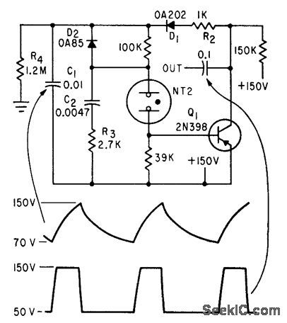
Operates over range of 0.05 to 7,000 cps by adjusting values of C1, C2, and R4. Average supply current drawn is less than 1 ma.-R. D. Ryan, Low-Cost Pulse Generator, Electronics, 35:15, p 70. (View)
View full Circuit Diagram | Comments | Reading(713)
POSITIVE_AND_NEGATIVE_VOLTAGE_POWER_SUPPLY
Published:2009/7/16 1:47:00 Author:Jessie
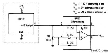
This circuit provides a precision voltage source that can be adjusted through zero to positive and nega-tive voltages, which eliminates reversing connections on the power supply. Also, it is possible to get exactly 0 V, without some offset.
As to how this circuit works, first consider the -1 V/V to + 1 V/V linear gain-control amp (see the figure). A Burr-Brown INA105 difference amp is used in a unity-gain inverting amp configuration. A potentiometer is connected between the input and ground.
The pot's slider is connected to the noninverting input of the unity-gain amp; this input is typically connected to ground. With the slider at the bottom of the pot, the circuit is a normal-precision unity-gain inverting amp witha gain of -1.0 V/V 10.01% maximum. Withthe slider at the top of the pot, the circuit is a normal-precision voltage follower with a gain of ±1.0 V/V ±0.001% maximum. With the slider in the center, there's equal positive and negative gain for a net gain of 0 V/V. The accuracy between the top and the bottom will usually be limited by the accuracy of the pot. (View)
View full Circuit Diagram | Comments | Reading(1279)
LEAD_ACID_BATTERY_TEMPERATURE_COMPENSATED_CHARGER
Published:2009/7/14 0:27:00 Author:May
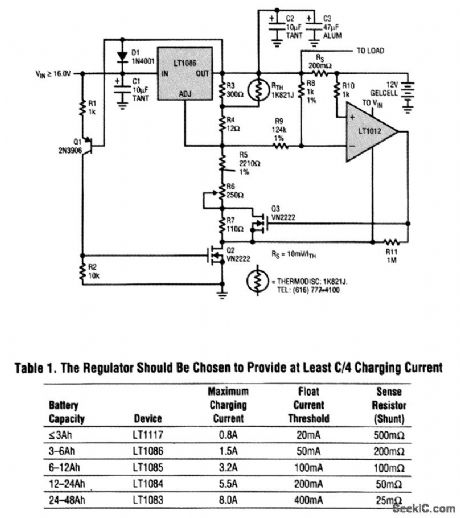
The charging characteristics of lead-acid cells are strongly linked to the ambient temperature. To prevent over-or undercharging of the battery during periods of extended low or high temperatures, temperature compensation is desirable. This circuit incorporates a low-dropout linear regulator, temperature compensation, dual-rate charging, and true negative ground, and consumes zero standby current. The LT1086 linear regulator is used to control the charging voltage and limit maxi-mum charging current. If the input supply is removed, Q1 and Q2 turn off and all charger current paths from the battery to ground are interrupted, resulting in zero shutdown current draw. Diode D1 provides reverse current flow protection for the regulator should the input fall below the battery voltage or be shorted. The temperature compensation employed in this circuit follows the true cur-vature of a lead-acid cell. Temperature compensation is provided by RTH, which is a Tempsistor, in parallel with R3. Changes in temperature alter the resistor divider ratio of the regulator. The match is within 100 mV for a 12-V battery over a range of -10 to +60℃. The best location for the Tempsistor is directly under the battery, with the battery resting on a pad of Styrofoam. Dual-rate charging is implemented by comparator LT1012, which senses the charging current through current-sense resistor RS. When the current is greater than 10 mV/RS, the high-rate charging voltage is 14.4 V at 25℃; when the current is less than this threshold, the float charging voltage is 13.8 V. (View)
View full Circuit Diagram | Comments | Reading(2095)
SIMPLE_CHARGER
Published:2009/7/14 0:11:00 Author:May
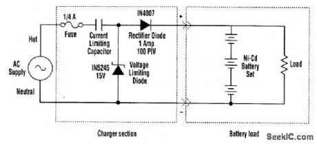
Built with just four components, this battery charger for small NiCd batteries is useful as a compact travel charger or in floating simple battery-backed projects. It is small enough to fit in a 35-mm film canister.Warning: This circuit is not isolctted from the ac line cmd presents a shock hazard if there is any contact between it and a person or another device. (View)
View full Circuit Diagram | Comments | Reading(998)
FLOAT_CHARGING_CIRCUIT
Published:2009/7/14 0:05:00 Author:May
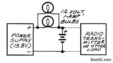
To float-charge a 12-V lead-acid battery, all you need is an accurately regulated 13.8-Vdc power supply. You could connect the power supply directly to the battery, but it is safer to make the connection through a couple of 12-V, 1-A automotive light bulbs. The light bulbs serve as current limiters; they guarantee that no matter what happens, the power supply will never have to deliver more than 2 A. Resistors can also serve as current limiters, but light bulbs are better because their resistance varies with current in a useful way. It's nearly zero at low current, but as the current through each bulb approaches 1 A the bulb lights and the resistance increases. Thus, the bulb limits the current, but doesn't waste energy when the current is low. This setup is a good way to power a heavy load that operates intermittently, such as a ham radio transmitter. The battery delivers heavy current when necessary and the power supply keeps the battery charged. (View)
View full Circuit Diagram | Comments | Reading(1000)
CONSTANT_CURRENT_NiCd_CHARGER
Published:2009/7/13 23:46:00 Author:May
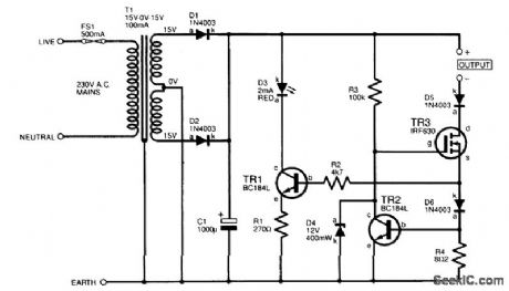
A tapped transformer(T1)with two rectifier diodes (D1 and D2) and capacitor C1 provides the primary dc supply from the 230 Vac The power MOSFET device TR3 is initially biased into conduction by a positive gate voltage from resistor R3 Current flowing through the load flows through Current-sensing resistor R4,developing a voltage When this reaches about 0.5 V, transistor TR2 begins to conduct,reducing the gate (g) voltage of TR3 The circuit stabilizes at the load current that gives 0.5 V across R4 Zener diode D4 prevents excessive gate voltage from being applied to power MOSFET TR3,which might happen if the circuit was powered without the load connected,Diode D6 compensates for the base-emitter voltage drop of transistor TR1 so that the voltage across R4 is duplicated across resistor R1,controlling the current flow through LED D3 The apparent brightness of LED D3 therefore depends on the charging current,so any problems with connection to the cells on charge will be immediately apparent to the user Diode D5 prevents any “back feeding” of current from the batteries power supply fails while the batteries are still connected (View)
View full Circuit Diagram | Comments | Reading(2744)
1_A_12_V_REGULATED_SUPPLY
Published:2009/7/16 1:44:00 Author:Jessie
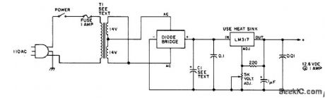
Using a junked VCR power transformer, this circuit supplies 12 V at 1 A. (View)
View full Circuit Diagram | Comments | Reading(742)
NEGATIVE_SUPPLY_FROM_A__12_V_SOURC
Published:2009/7/16 1:42:00 Author:Jessie
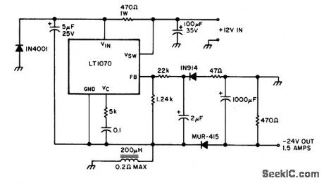
This switching regulator will produce a -24-V/1.5-A source from a +12-V supply, for applications where a positive-grounded source is necessary. (View)
View full Circuit Diagram | Comments | Reading(726)
__24_V_15_A_SUPPLY_FROM_A___12_V_SOURCE
Published:2009/7/16 1:41:00 Author:Jessie
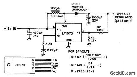
This switching regulator will produce 1.5 A at 24 V from a 12-V auto battery. It operates as a boost-switching supply using an LT 1070. The diode should be a fast-switching type because this regulator operates above 10 kHz. (View)
View full Circuit Diagram | Comments | Reading(1475)
| Pages:74/291 At 206162636465666768697071727374757677787980Under 20 |
Circuit Categories
power supply circuit
Amplifier Circuit
Basic Circuit
LED and Light Circuit
Sensor Circuit
Signal Processing
Electrical Equipment Circuit
Control Circuit
Remote Control Circuit
A/D-D/A Converter Circuit
Audio Circuit
Measuring and Test Circuit
Communication Circuit
Computer-Related Circuit
555 Circuit
Automotive Circuit
Repairing Circuit