
power supply circuit
Index 72
SELF_STABILIZING_ZENER
Published:2009/7/15 21:08:00 Author:Jessie
Current through 7.5-mA zener CR1 is independent of supply volt-age, which may be as low as 10V. Negative reference is 1.1 times zener rating, or -6.8 V for zenel shown. Article describes circuit operation and gives design equations.-L. Accardi, Super-Stable Reference-Voltage Source, EDN/EEE Magazine, Oct. 1, 1971, p 41-42. (View)
View full Circuit Diagram | Comments | Reading(885)
±7_V_REFERENCE
Published:2009/7/15 22:13:00 Author:Jessie
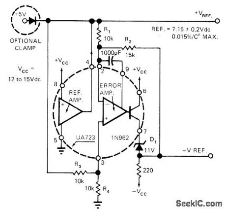
Developed for analog applications requiring dual-polarity references. Both voltages are generated from single μA723 IC voltage regulator chip. Chief requirement is keeping inputs and outputs within dynamic range of amplifier, which is +2 to +9 V; this is done by shifting output voltage level upward with zener D1 and shifting input error voltage with divider R1-R2. Changing ratio of R3 to R4 changes negative reference value.-D. Weigand, Dual 7V Reference Developed from a Single μA723, EDN Magazine, Nov. 1, 1972, p 47. (View)
View full Circuit Diagram | Comments | Reading(883)
_66_V_AT_5_mA
Published:2009/7/15 21:33:00 Author:Jessie

Half of 1558 dual opamp is used as buffer for basic opamp-zener voltage reference to raise output current and lower output impedance-W. G. Jung, IC Op-Amp Cookbook, Howard W Sams, Indianapolis, IN, 1974, p 150-151. (View)
View full Circuit Diagram | Comments | Reading(948)
FOUR_ELECTRODE_NEON
Published:2009/7/15 21:32:00 Author:Jessie
On-off indicator for transistorized flip-flop operates on voltage differential of 6V.-A. Erikson, French Components Gaiting Smaller, Electronics, 34:11, p 24-25. (View)
View full Circuit Diagram | Comments | Reading(733)
_66_V_WITH_741_OPAMP
Published:2009/7/15 21:32:00 Author:Jessie
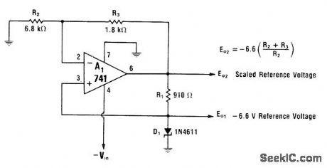
Reference output of -6.6 V, determined by breakdown voltage of zener, is scaled to more negative level at output of A1. If 1558 dual opamp is used in place of 741, other section can be connected to zener as buffer that raises output current to 5 mA and lowers output impedance.-W. G. Jung, IC 0p-Amp Cookbook, Howard W. Sams, Indianapolis, IN, 1974, p 151. (View)
View full Circuit Diagram | Comments | Reading(1335)
VARIABLE_25_10_V
Published:2009/7/15 21:31:00 Author:Jessie
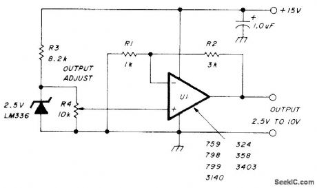
General-purpose opamp and tenet, operating from single 15 V supply, serve as stable buffered voltage reference source that is readily adapted to wide range of output voltages and currents. R4 applies some fraction of zener's 2.5 V to opamp, which amplifies it by factor of 4 to give 2.5 to 10 V output. Output current rating depends on opamp and is about 10 mA for general-purpose types. 759 will handle up to 350 mA, and other devices can be buffered with NPN emitter-follower stage. For greater output range, use higher supply voltage and ad just R2 accordingly. R3 should be chosen to maintain about 1 mA in zener.-W. Jung, An IC Op Amp Update, Ham Radio, March 1978, p 62-69. (View)
View full Circuit Diagram | Comments | Reading(1813)
10_V_HIGH_PRECISION
Published:2009/7/15 21:24:00 Author:Jessie
Use of LM399 thermally stabilized subsurface zener in state-of-the-art reference circuit keeps temperature error well under 2 PPM/℃ over temperature range of 0 to 70℃. Article gives design equation and covers procedures for optimizing stability and minimizing power-supply rejection-ratio errors.-W. G. Jung, Precision Reference Source Features Minimum Errors, EDN Magazine, Aug. 5, 1976, p 80 and 82.
(View)
View full Circuit Diagram | Comments | Reading(2797)
KILOVOLT_PULSES
Published:2009/7/15 21:23:00 Author:Jessie
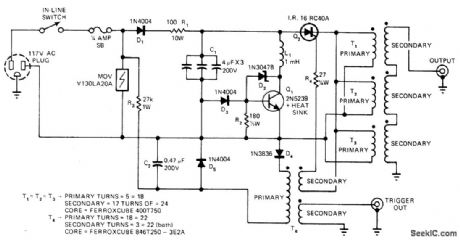
Simple circuit generates 1.5-kV pulses at fixed rate equal to line frequency. Used to drive small piezoelectric transducers for sound velocity measurements. Absence of power transformer minimizes cost, size, and weight. During half of AC cycle, C1 charges. During other half, C1 discharges through Q2 into primaries T1, T2, and T3 to provide output pulse. R3, C2, D5, D4, and T4 provide trigger pulse for turning on Q2. Shunt regulator formed by D2, D3, R2, Q1, and L1 clamps voltage across C1 at 130 V to ensure constant amplitude of output pulses.-S. Anderson, Portable Generator Produces Kilovolt Pulses, EDN Magazine, Oct. 20, 1977, p 102. (View)
View full Circuit Diagram | Comments | Reading(928)
BUFFERED_10_V
Published:2009/7/15 21:23:00 Author:Jessie
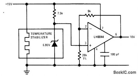
Reference voltage developed by National LM199 temperature-stabilized IC is 6.95 V with very low temperature drift and excellent long-term stability. LH0044 precision low-noise opamp is used to scale and buffer reference to give required output of 10 V. Regulation of 15-V supply need be only about 1%.- Linear Applications, Vol. 2, National Semiconductor, Santa Clara, CA, 1976, AN-161, p 5. (View)
View full Circuit Diagram | Comments | Reading(1016)
_10000_V
Published:2009/7/15 21:22:00 Author:Jessie
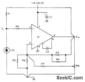
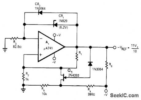
Uses LM301A opamp with 1N825 6.2-V zener reference diode (not zener regulator diode) to maintain stable DC voltage under severe combinations of temperature, shock, and vibration. Gain resistors R2 and R3 should have same 0.01%/℃ temperature coefficients as reference diode. R1 is RN55 511-ohm metal-film resistor, R2 is RN55E 6.04K metal-film resistor, and R3 is RN55E 3.57K metal-film resistor. R4 and R5 are gain trim resistors. R6 should equal parallel combination of R2 and R5. R8 is 10K cermet pot. with R7 (optional) 100K to 1 megohm. Article tells how to trim circuit for desired out-put and how to calculate values of resistors and temperature coefficients for other output volt-ages.-D. W. Ishmael, Precision +10.000 V DC Voltage Reference Standard, 73 Magazine, Sept. 1975, p 124-126. (View)
View full Circuit Diagram | Comments | Reading(1359)
34_V_RADIATION_HARD_ENED
Published:2009/7/15 21:20:00 Author:Jessie
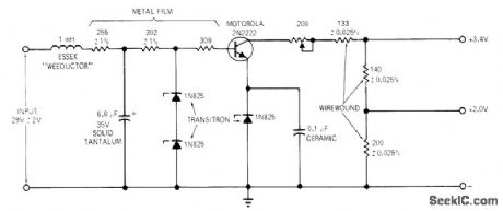
Two-stage regulator is combined with special filter design that helps keep output voltage free of gamma-produced transients and RFI. Voltage divider using wirewound resistors provides 2-V output. Gamma radiation of 1,000,000 rads caused only 0.3% change in output voltages. Article covers procedure for designing and testing circuits that are to be operated in high-radiation environment.-A. J. Sofia, Designing a Radiation-Stable Voltage Reference, EDN Magazine, Sept. 15, 1970, p 39-41. (View)
View full Circuit Diagram | Comments | Reading(859)
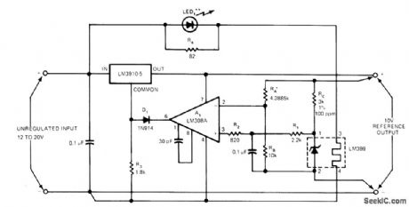
_10__20_AND__30_V
Published:2009/7/15 21:34:00 Author:Jessie
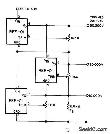
Simple stacking arrangement of Precision Monolithics REF-01 voltage references gives near-perfect line regulation for inputs of 32 to 60 V, with output changes less than noise voltage of devices for input extremes. Any number of units can be stacked to obtain additional output voltages.- + 10 V Precision Voltage Reference, Precision Monolithics, Santa Clara, CA, 1977, REF-01, p 7. (View)
View full Circuit Diagram | Comments | Reading(884)
TRANSIENT_IMMUNE_SCR_LATCHING_CIRCUIT
Published:2009/7/15 22:58:00 Author:Jessie
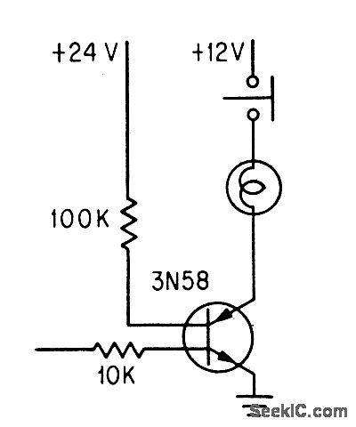
With 100,000-ohm resistor of silicon controlled switch returned to +24 v, latching circuit for lamp is immune to transient spikes of up to 12 v as well as to rate effect when turned off.-R. A. Stasior, How to Suppress Rate Effect in PNPN Devices, Electronics, 37:2, p 30-33. (View)
View full Circuit Diagram | Comments | Reading(946)
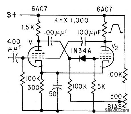
PRF_GENERATOR
Published:2009/7/15 22:48:00 Author:Jessie
Provides frequency stability of 3% as repetition rate generator in airborne radar. Free-running connections are shown, but may also be triggered externally.-NBS, Handbook Preferred Circuits Navy Aeronautical Electronic Equipment, Vol.1, Electron Tube Circuits, 1963, p N5-1. (View)
View full Circuit Diagram | Comments | Reading(1039)
PROGRAMMABLE_CONTROLLER_PHOTOELECTRIC_INTERFACE
Published:2009/7/15 22:46:00 Author:Jessie
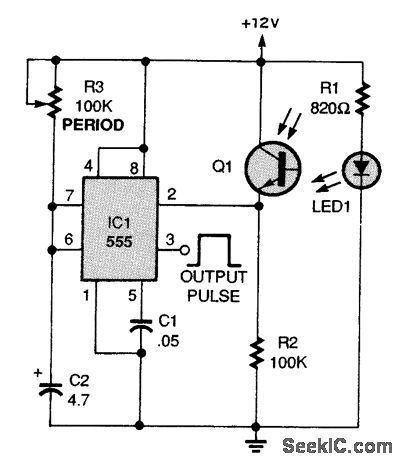
This circuit is an IR sensor with a timed positive output pulse that will operate with older and slower PLCs. Some of the early PLCs have scan times of 15 ms or more. The sensor's extended output pulse can be set, by R3, to a time period longer than the controller's scan time, The sensor can also be used as a stand-alone circuit to operate a counter, a valve, an indicator, or any other electrically controlled device. As long as nothing is blocking the IR light source, the emitter of phototransistor Q1 is high and 555 timer IC1 is set in the READY state. When an object blocks the light source, Q1 turns off, sending a negative pulse to the trigger input at pin 2 of IC1, producing a timed output pulse. R3, and C2, determine the length of the output pulse. Larger values produce longer output pulses. (View)
View full Circuit Diagram | Comments | Reading(1006)
HIGH_TRIGGERING_SENSITIVITY
Published:2009/7/15 22:20:00 Author:Jessie
Semiconductor diode is used as series nonlinear element in feedback loop of monostable mvbr, to give good stability along with improved triggering sensitivity for nuclear event registration, pulse analysis, counting, and time modulation.-M.M. Voiinovic, Series Diode Increase Multivibrator Sensitivity, Electronics, 32:17, p 90-91. (View)
View full Circuit Diagram | Comments | Reading(891)
OPAMP_AS_MILLIVOLT_REFERENCE_1
Published:2009/7/15 22:20:00 Author:Jessie
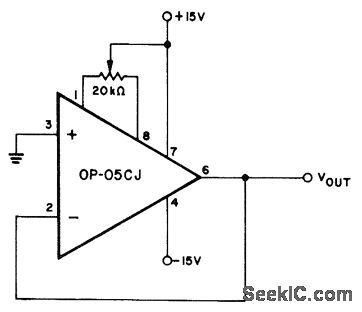
High-performance bipolar-input Precision Monolithics OP-05CJ instrumentation opamp is connected as unity-gain buffer. Output is adjusted to desired reference voltage with pot connected to offset nulling terminals. Reference range is -3.5 mV to +3.5 mV, and long-term drift of zener less source is less than 3.5 μV per month.-D. Soderquist, Simple Precision Millivolt Reference Uses No Zeners, Precision Monolithics, Santa Clara, CA, 1975, AN-10. (View)
View full Circuit Diagram | Comments | Reading(1555)
2_Hz_TO_1_MHz
Published:2009/7/15 22:19:00 Author:Jessie
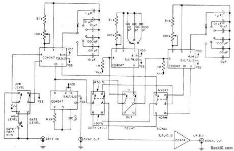
General-purpose laboratory pulse generator uses four CD4047A MVBRs to provide six overlapping ranges of frequencies along with pulse-width control, delayed sync, and gating from high-level or low-level input. When delay switch is IN, MVBR at upper center produces variable output delay from 1.5 μs to 250 ms with respect to sync pulse. When delay pulse is OUT, this mono MVBR is bypassed and inherent delay is then about 400 ns. Signal output is buffered with CD4041A for driving any required load. Supply voltage is not critical and can be taken from device under test.- COS/ MOS Integrated Circuits, RCA Solid State Division, Somerville, NJ, 1977, p 619-620. (View)
View full Circuit Diagram | Comments | Reading(1923)
OPAMP_AS_MILLIVOLT_REFERENCE
Published:2009/7/15 22:19:00 Author:Jessie
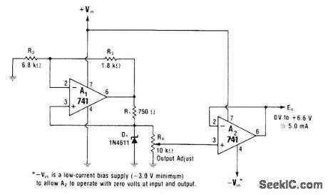
R4 at input of voltage-foilower opamp permits varying ref erence voltage from 0 up to limit of zener. A2 compensates for loading of zener by R4. Dual opamp cannot be used because negative supply terminal of A2, must be slightly more negative than -3 V common to permit linear output operation down to 0 V. If additional load current is required, NPN booster transistor can be used with A2.-W. G. Jung, IC Op-Amp Cookbook, Howard VV, Sams, Indianapolis, IN, 1974, p 155-157. (View)
View full Circuit Diagram | Comments | Reading(1463)
MEMORY_REFRESHER
Published:2009/7/15 22:17:00 Author:Jessie
Delivers high-energy pulses in extremely low duty-cycle mode. Developed to provide memory-refresh pulses for MOS memory system from standby battery. Circuit is basically programmable UJT oscillator with divider R2-R3 setting threshold or trigger level. To complete one cycle and start next, UJT is turned off by zener. Current through L1 drops, and resulting negative transient at base of Darlington outs it off. This generates high-power pulse with very sharp rise and fall times. Charging sequence then starts again to give sustained oscillation. Article gives design equations.-J. P. Stein, PUT Delivers Ultra-Low-Power. High-Energy Pulses, EDN Magazine, Sept.1, 1972, p 51-52. (View)
View full Circuit Diagram | Comments | Reading(1429)
| Pages:72/291 At 206162636465666768697071727374757677787980Under 20 |
Circuit Categories
power supply circuit
Amplifier Circuit
Basic Circuit
LED and Light Circuit
Sensor Circuit
Signal Processing
Electrical Equipment Circuit
Control Circuit
Remote Control Circuit
A/D-D/A Converter Circuit
Audio Circuit
Measuring and Test Circuit
Communication Circuit
Computer-Related Circuit
555 Circuit
Automotive Circuit
Repairing Circuit