
power supply circuit
Index 75
TIMED_NiCd_CHARGER
Published:2009/7/13 23:29:00 Author:May
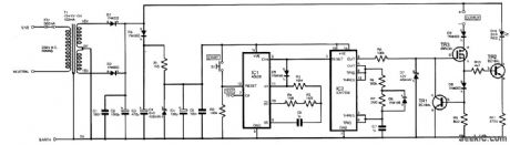
The primary supply is provided by 230 V through transformer T1, diodes D1 and D2, and reservoir capacitor C2. A supply for the timing circuit is provided through diode D3, with resistor R1 and zener diode D4 to keep it to a safe voltage for the CMOS devices used. These CMOS devices, IC1 and IC2, use so little current that the timer will keep going for up to 30 s if the power fails, preventing the charge period from being restarted by every minor glitch in the supply. IC1 is a 4060B 14-stage divider with built-in oscillator. Pressing switch S1 sets all its outputs low, so diode D5 is reverse-biased and the oscillator operates. With the component values shown, it runs at about 0.17 Hz, so the last output of the divider, pin 3, goes high after about 14 h. This applies forward bias to D5, which stops the oscillator. The first timer of the 7556 dual CMOS timer IC2 is connected to operate as an oscillator with a frequency of about 0.5 Hz with a duty cycle of about one to five. Pin 4 is an active low reset for this timer, so although the input to this from IC1 is low, its output is also low. The second timer is used as an inverter to convert this to a high output, which, via resistor R8, activates the output constant-current generator. When IC1 times out, the oscillator in IC2 starts running, and the current generator is then pulsed for about 400 ms every 2 s. NiCds have quite a high self-discharge rate: about 10 percent of capacity per week. If left on this charger, they will be kept fully topped up ready for use without overcharging, and by flashing in time with the current pulses, LED D10 will let the user know that the main charge period is complete
(View)
View full Circuit Diagram | Comments | Reading(1062)
3_A_BATTERY_CHARGER_FOR_Li-ION_OR_NiCd
Published:2009/7/13 23:22:00 Author:May
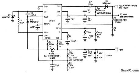
The LT1511 implements the constant-voltage/constant-curren t profile required for lithium-ion (Li-ion) batteries. It can also charge nickel-cadmium (NiCd) and nickel-metal-hydride (NiMH) batteries by using an extemal charge-termination method. Full charging current can be programmed by resistors or a DAC. An input current regulating loop on the LT1511 allows simultaneous equipment operation and battery charging without overloading the wall adapter. The charging current is automatically reduced to keep the wall adapter current within specified levels. (View)
View full Circuit Diagram | Comments | Reading(1013)
CURRENT_SUPPLY_FOR_RTTY_MACHINES
Published:2009/7/16 1:38:00 Author:Jessie
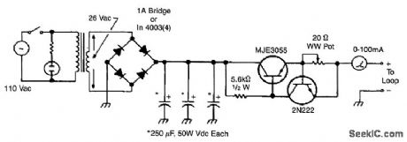
Suitable for powering an old Model 15 Teleprinter, this simple simple to construct. The 20-Ω pot adjusts loop current. (View)
View full Circuit Diagram | Comments | Reading(790)
3_TO_15_V_dc_dc_CONVERTER
Published:2009/7/16 1:37:00 Author:Jessie
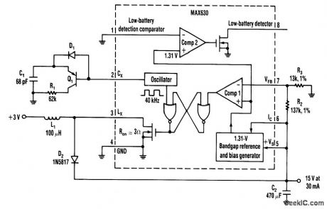
This circuit supplies 15 V at 30 mA from a 3-V source. The MAX630 IC is dc-dc converter, Q1 and D1 modify the duty cycle from 50% to 80% to optimize the output power. (View)
View full Circuit Diagram | Comments | Reading(747)
PRECISE_LOW_CURRENT_SOURCE
Published:2009/7/16 1:35:00 Author:Jessie
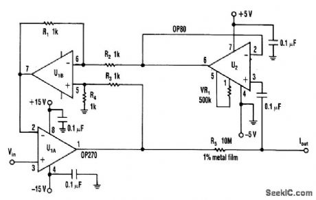
A current source that attains a resolution as low as 10 pA is useful in applications where a precise, low-value current is needed. When the circuit forces current into ground, the output remains within 2% of the ideal current over the ±100-nA range. Over the -4- to +3.5-V compliance range, the error that appears is less than 5%. This accuracy results from using an OP80 op amp from Precision Monolithics in the feedback loop. The OP80 has an IB of 200 mA typical.
For a given voltage (Vin), amp U1A generates an output voltage so that the current through R5 equals Vin divided by R5 (10 MΩ). This current causes a voltage drop across R5, which is sensed by the unity-gain differential amp (U1B and U2). That amp's output is connected to the inverting input of U1A, completing the feedback loop.
The noise in the circuit is of particular concern, especially that produced by resistor R5. The circuit is limited to low-frequency and dc applications as a result of its 400-n V/kHz noise. For applications that don't require the circuit's 10-pA output, lower values of R5 can be substituted. This will increase the bandwidth.
(View)
View full Circuit Diagram | Comments | Reading(1623)
±35_V_SUPPLY_FOR_AUDIO_AMPLIFIERS
Published:2009/7/16 1:30:00 Author:Jessie
This supply will be found useful for operating 100-W output range. T1 = 120 V: 70 V CT at 5 A. (View)
View full Circuit Diagram | Comments | Reading(811)
STEP_UP_SUPPLY_BATTERY_CHARGER
Published:2009/7/13 23:16:00 Author:May
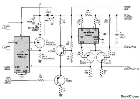
IC1 is a step-up switching regulator that boosts Vin (nominally 5 V) as necessary to supply the combination of charging current and load current. The 5-V source must include short-circuit protection. IC2 is a high-side current-sense amplifier that monitors the charging current. Commands from the processor include. CHARGE ON/OFF and FAST/TRICKLE CHARCGE. IC2 produces an output current (OUT) equal to 10-4 of the current through sense resistor R9. Q3 and Q4 are on during a fast-charge operation, so this output current flows through the parallel combination of R11 and (approximately) R4. The resulting feedback to IC1 (pin 3) maintains the fast-charge current through R9 at 500 mA. This feedback also enables the regulator to supply as much as 500 mA of load current in addition to the fixed 500 mA of charging current. Q2 limits the battery voltage to 10 V (2 V/cell). During the fast charge, an external processor and multichannel A/D converter (ADC) must monitor the battery's terminal voltage. When the ADO senses a change of slope in this voltage, the processor terminates the fast charge by asserting a high on FAST/TRICKLE CHARGE. Q3 turns off, causing a rise in the feedback (FB) that lowers the charging current to the trickle charge rate (approximately 60 mA). If IC1 shuts down or if the load current plus charging current exceeds the capability of IC1, the R9 current reverses as current flows out of the battery. IC2 indicates the reversal by allowing R13 to pull its open-collector SIGN output high, turning off Q4 and turning on Q5. Current through R12 then produces a voltage proportional to the battery's discharge current (5 A through R9 produces a full-scale response of 3 V across R12). By integrating this voltage over time (sampling at fixed intervals and multiplying by the time interval), the A/D-processor system can monitor energy removed from the battery. Based on this measurement and the terminal-voltage measurement, the processor can then reinitiate a fast charge (by asserting FAST/TRICKLE CHARGE low) before the battery reaches its end of life.
(View)
View full Circuit Diagram | Comments | Reading(1568)
BRIDGE_RECTIFIER
Published:2009/7/16 1:29:00 Author:Jessie
This bridge circuit is intended for those cases where two unequal supply voltages are required. The lower voltage is obtained with the aid of a transformer with symmetric windings and half-wave rectification of the potential across one winding.
For the higher voltage, the potential across both windings is rectified. To that end, the output of the transformer is linked to the bridge rectifier via two electrolytic capacitors that provide isolation of the two direct voltages.
A bonus with this type of circuit is that although the two supplies can be loaded unequally, the currents through the two transformer windings are the same. Thus, the transformer is loaded symmetrically so that its full capacity can be used. Moreover, no unnecessary dissipation is in the voltage regulators.
The load on the lower voltage supply depends primarily on the rating of the transformer. The load on the higher voltage supply is limited by the reactance of C1 and C2 ( 1/2π 50 C) and the required minimum output voltage.
(View)
View full Circuit Diagram | Comments | Reading(1513)
NEGATIVE_VOLTAGE_FROM_A_POSITIVE_SUPPLY
Published:2009/7/16 1:25:00 Author:Jessie
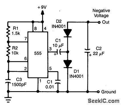
By using a 555 timer to generate a square wave and voltage-doubling the output, a negative voltage that is almost equal to the positive supply can be obtained. The current available is up to 20 to 30 mA or so, depending on the regulation and voltage needed. (View)
View full Circuit Diagram | Comments | Reading(1518)
BATTERY_TRICKLE_CHARGER
Published:2009/7/13 23:08:00 Author:May
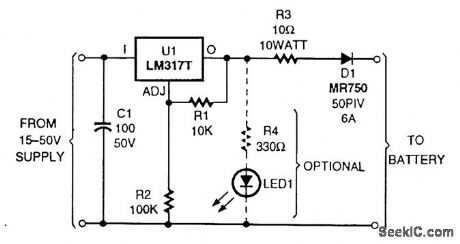
The circuit is built around an LM317T adjustable voltage regulator. Its output voltage (VOUT) is determined by the formula VOUT= l.25 (1+R2/R1). I chose a 10-kΩ resistor for R1 and a 100-kΩ resistor for R2 to allow for a little wasted current flow (around 125 μA). This will develop 13.75 V between the output terminal and ground. R3 and a diode prevent burnout if the terminals are shorted or reversed, and prevent battery discharge in the event that the regulator is disconnected from the main power supply. The capacitor is optional but will make life easier on the chip under an extreme charging cycle. With proper heat sinking, the IC is capable of carrying 1.5 A to the battery. The circuit can be left hooked to the battery all of the time and will not overcharge it. (View)
View full Circuit Diagram | Comments | Reading(2534)
MORE_EFFICIENT_BATTERY_CHARGER
Published:2009/7/13 22:57:00 Author:May
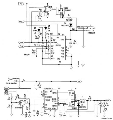
The project at hand was to build a small, efficient, inexpensive, full-function battery charger that could charge 2 to 10 NiCd or NiMH cells. A switching regulator that could be set up as a constant-current source was needed. Connecting the negative end of the battery directly to ground provides more voltage and reduces IR losses. Linear Technology's LTC1148HV synchronous step-down switching regulator fills this role because it is more than 90 percent efficient, and it features two current sense inputs (Sense+ and Sense-) and a current control pin (Ith) that has a dc input linearly related to the maximum coil current (Fig. 1). For example, with a low, commonly available 0.1-Ω sense resistor and Ith connected to the 2-JV reference output of the MAX713, the peak coil current is set to 1.55 A. The average current will still vary with output voltage, but this can be compensated for by feeding back some of the output voltage to Ith The constant-voltage regulation loop of the LTC1148 is disabled once the voltage divider (R2 and R7) forVFB is set above the highest voltage that the battery is going to reach during charge. With the battery above the constant voltage regulation point, the switching regulator will supply no current. If a trickle charge current is desired, a switch (USA) and a resistor (R14) can be added that supply the desired current directly from the primary dc source (Vin)-a simple wall cube-when the MAX713 controller terminates fast charge or during battery undervoltage condition at startup. (View)
View full Circuit Diagram | Comments | Reading(1488)
BATTERY_CHARGER
Published:2009/7/13 22:39:00 Author:May
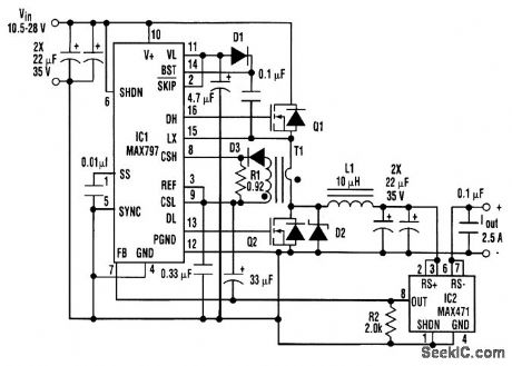
This current-source battery charger can source 2.5 A with up to 96 percent efficiency. It can operate from an ac adapter or directly from a car battery. By sensing current on the high side of the battery being charged, it preserves the low impedance of the automobile's ground-return system. The charger handles battery stacks of 5 to 15 cells, and its input voltage can range from 28 V down to a level 1.5 V above the terminal voltage of a fully charged battery. Charging current is generated by the current-mode, buck-regulator controller IC1, operating with an external power switch (Q1) and a synchronous rectifier (Q2). Both are N-channel MOSFETs, whose low on-resistance (vs. P-channel types) contributes to high efficiency in the circuit. The IC includes a charge pump for generating the required positive gate voltage for Q1. It also senses the Q1 current (via R1) and shuts down if this current becomes excessive.The current-sense transformer (T1) saves power by diverting a fraction of Q1's current through R1. Operating on the output's high side is the current-sense amplifier IC2. Its OUT current (1/2000 of the current flowing internally from RS+ to RS-) flows through R2 to produce a feedback signal for IC1. Digital control of the charging current can be introduced by switching among different-switching FETs like the 2N7002; its 7.5-Ω on-resistance is not a problem because its drain current-no greater than 1.25 mA-introduces an error no greater than 0.5 percent. Circuit efficiency ranges up to 96 percent. Efficiency and power output both increase with output voltage, because the circuit's power consumption (associated mainly with IC1 and the switching MOSFETs) is almost constant. This buck regulator's output cannot rise about Vin in most cases, overvoltage protection is not required. VOUT which supplies power to IC2, must not go below 4 V. (View)
View full Circuit Diagram | Comments | Reading(0)
90_PERCENT_EFFICIENT_FOUR_CELL_NiCd_CHARGER
Published:2009/7/13 22:31:00 Author:May
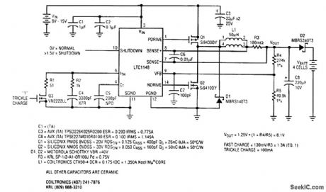
An embedded battery charger requires extremely low power dissipation in order to minimize heat buildup in compact portable systems. This schematic shows a charger that can charge four NiCd cells and is selectable for either a 1.3-A fast charge or a 100-mA trickle charge with up to 90 percent efficiency. The LTC1148 is a step-down synchronous switching regulator; it controls the charge rate, monitoring the output current via external current-sense resistor R3. Fast charge current is determined by the value of R3, according to the fast charge equation. In this case, it is set to 1.3 A. The resistor divider network R4 and R5 sets the output voltage to a nominal 8.1V under noload conditions, such as when the battery is removed. A four-cell NiCd pack's voltage will range from 3.6 to 6 V, depending upon its state of charge. When installed, the battery will pull the output below 8.1 V and place the LTC1148 into current-limited operation at 1.3 A. This constant current will be delivered until trickle charge is enabled by an external charge termination circuit or the battery is removed. Q3 enables trickle charge operation with charge current set by choice of R1. Diode D2 prevents the battery from being drained by the feedback resistor network when the LTC1148 is shut down.
(View)
View full Circuit Diagram | Comments | Reading(1074)
PRECISION_Li-ION_BATTERY_CHARGER
Published:2009/7/13 22:14:00 Author:May

An alternative to using expensive 0.25-percent precision resistors is presented in this battery-charger design, which adds two 1-percent resistors and two jumpers to the charger.In constant-voltage-mo de charging, a lithium-ion cell requires 4.1 V ±50 mV. The 1.2-percent requirement represents a tight tolerance. In a regulation loop where a voltage divider is compared against a reference, the accuracy is typically achieved by selecting a 0.7-percent reference and a volt-age divider with 0.25-percent tolerance resistors. Unfortunately, 0.25-percent precision resistors cost three times as much as 1-percent resistors and have very long lead times. One solution for moderate-volume production involves adding two 1-percent resistors and two jumpers to the charger circuit (see the figure). The jumpers are removed as necessary to bring the constant voltage to the required accuracy of 1.2 percent. The charger selected for this example is the LT1510. There are three lithium-ion cells in the. battery. After a value is selected for R4 the values for R1, R2, and R3 can be calculated using the equations given. K is the relative change required for a circuit with all of its tolerances in one direction. For example, in the case of a 0.5-percent reference and two 1-percent resistors, the total tolerance is 2.5 percent. To bring it back to 1.2 percent, the percentage change required is 2.5 percent - 1.2 percent 1.3 percent, and K =0.013. The jumpers (J1 and J2) must be opened based on the following:If VOUT is K/2 below nominal, remove J1.If VOUT is K/2 above nominal, remove J2.The following values were calculated: R1 = 4.99 kΩ, R2 = 324Ω,R 3=80.6 ,Ω and R4= 20 KΩ The voltage below which jumper J1 should be opened is 12.34 V -1.3 percent /2 = 12.22 V. The voltage above which jumper J2 should be opened is 12.34 V + 1.3 percent /2 = 12.42 V. (View)
View full Circuit Diagram | Comments | Reading(1849)
AUXILIARY_NEGATIVE_dc_SUPPLY_FOR_BIAS_OR_REFERENCE_APPLICATIONS
Published:2009/7/16 1:55:00 Author:Jessie
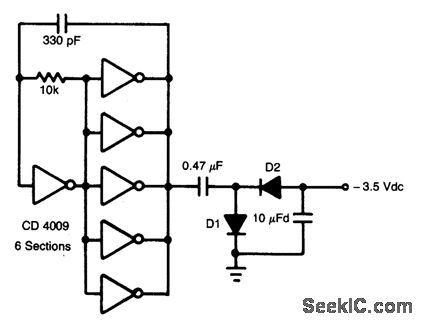
In this circuit, IC1 (CD4009) is used as a square-wave oscillator at approximately 25 kHz. C1 and R1 set this frequency. C2, D1, D2, and C3 form a p-p rectifter, which outputs about -3.5 Vdc. This circuit should be useful where a small negative dc supply is required, but only positive dc voltages are available. (View)
View full Circuit Diagram | Comments | Reading(1149)
5_AND±12_V_ac_POWERED_SWITCHING_SUPPLY
Published:2009/7/16 1:54:00 Author:Jessie
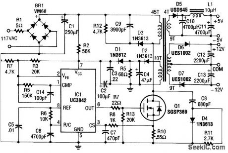
This supply uses an SGS-Thomson UC3842 IC in an off-line flyback regulator, providing + 5 V at 4 A and± 12 V at 300 mA. This enables a small high-frequency (50 kHz) transformer, to handle large amounts of power that are normally handed by a 60-Hz transformer. Q1 is a 5-A 500-V MOSFET, and the diodes are fast-recovery types. T1 has a 45-turn primary winding of #26 wire. The 12-V windings are each 9 turns of #30 wire, bifilar wound. The 5-V winding is 4 turns of four bifilar #26 wires. The control (feed-back) winding is two bifilar, parallel10-turn, #30 windings. The core is Ferroxcube EC35-3C8 with a 3/8 center leg. (View)
View full Circuit Diagram | Comments | Reading(7209)
POSITIVE_AND_NEGATIVE_VOLTAGE_SWITCHING_SUPPLY
Published:2009/7/16 1:51:00 Author:Jessie
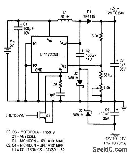
The LT1172 is configured as a step-up converter. C2 is charged by L1 and discharges into C4 when the LT1172's power switch goes to ground. Resistor R3 adjusts the output voltage between -12 and -24 V. (View)
View full Circuit Diagram | Comments | Reading(1866)
SCANNING_ADAPTER
Published:2009/7/13 5:22:00 Author:May

Developed for use with 2-meter transceiver having frequency synthesizer to provide automatic scanning that is disabled when transmitting and when receiver squelch is opened by transmission on one of channels being scanned. Will hang on to channel about 5 s after scanning is disabled, to allow starting of other side of communication. Scan rate is about 250 ms per channel. U1A generates 0 output when squelch is open, producing output of 1 for U1B that disables oscillator U1C-U1D, Oscillator drives D flip-flop that turns on Q1 and Q2 alternately. When Q1 is on, LED1 is lit to indicate that secondary channel is enabled, Article covers method of increasing number of scanned channels.-B. McNair, Add-a-Scanner, 73Magazine, Nov. 1978, p 116-119. (View)
View full Circuit Diagram | Comments | Reading(898)
HIGH_COMPLIANCE_CURRENT_SOURCE
Published:2009/7/13 5:05:00 Author:May
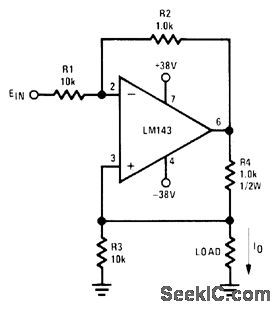
Non-inverting input of LM143 high-voltage opamp senses current through R4 to establish output current that is proportional to input voltage. With ±38 V supply, compliance of current source is ±28V. - Linear Applications, Vol. 2, National Semiconductor, Santa Clara, CA,1976, AN-127,p3. (View)
View full Circuit Diagram | Comments | Reading(1044)
4_20_mA_SOURCE
Published:2009/7/13 5:04:00 Author:May
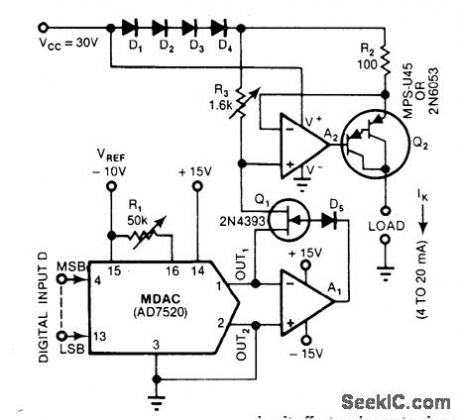
DigitaI input to multiplying digital-to-analog converter determines load current in range of 4 to 20 mA with 15.6-μA resolution. R1 adjusts ratio of full-scale to zero-scale current at output 1 of MDAC and R3 sets circuit offset and span to give correct end-range currents for load. Maximum load compliance is 25 V. Opamp types are not criticaL-J. Wilson and J. Whitmore, MDAC's Open Up a New World of Digital-Control Applications, EDN Magazine, Sept. 20, 1978, p 97-105. (View)
View full Circuit Diagram | Comments | Reading(1530)
| Pages:75/291 At 206162636465666768697071727374757677787980Under 20 |
Circuit Categories
power supply circuit
Amplifier Circuit
Basic Circuit
LED and Light Circuit
Sensor Circuit
Signal Processing
Electrical Equipment Circuit
Control Circuit
Remote Control Circuit
A/D-D/A Converter Circuit
Audio Circuit
Measuring and Test Circuit
Communication Circuit
Computer-Related Circuit
555 Circuit
Automotive Circuit
Repairing Circuit