
power supply circuit
Index 62
Regulator DC-DC Circuit and Pin of Power Supply Monitor and its Main Features TA78DS05P Regulator
Published:2011/9/3 22:42:00 Author:Zoey | Keyword: Regulator, DC-DC Circuit, Pin of Power Supply Monitor, Main Features

The TA78DS05P and TA78DS10P three-terminal regulators can output fixed low-margin voltage, the maximum current output is 30mA, and in a spare state, the typical voltage will be 500μA. The minimum output voltage margin is below 0.3V, and the maximum input voltage is 29V and the power is 800mW. The working temperature varies from -40 to +85℃.This circuit itself has interior overcurrent, overtemperature and short circuit- proof devices, as soon as the voltage exceeds 60V, the power supply will be cut off.
(View)
View full Circuit Diagram | Comments | Reading(628)
The regulator: DC-DC circuit, power supply monitor pin and its main features LM168/268/368
Published:2011/8/30 2:18:00 Author:Seven | Keyword: DC-DC circuit, power supply, monitor pin

LM168/268/368--the Vref circuitThis is a high-precision and low temperature drift 3-stage Vref circuit of temperature compensation; its output voltage can be 10, 6.2 or 5.0V, which can be regulated by ASJ; it works in the parallel or serial way; the output voltage fault typical value is ±0.02%; the input voltage typical value is 0.0001%/V; the working current range is 0.4~10mA; when the power supply current is 0~10mA, the typical value of load stability is 0.003%/mA; the max input voltage is 35V; the max forward current is 50mA; the power consumption is 600mW.
(View)
View full Circuit Diagram | Comments | Reading(674)
The regulator: DC-DC circuit, power supply monitor pin and its main features LM140/140A/340/340A
Published:2011/8/30 1:32:00 Author:Seven | Keyword: DC-DC circuit, power supply, monitor pin
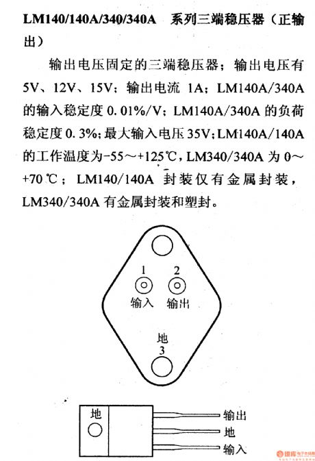
LM140/140A/340/340A--the 3-terminal stabilizer (positive output)This is a 3-terminal stabilizer with fixed output voltage; the output voltage can be 5V, 12V or 15V; the output current is 1A; the stability of LM140A/340A is 0.01%/V; the load stability of LM140A/340A is 0.3%; the max input voltage 35V; the working temperature of LM140A/140A is -55~+125℃ and that of LM340/340A is 0~+70℃; LM140/140A is only in metal package. LM340/340A is in metal or plastic package.
(View)
View full Circuit Diagram | Comments | Reading(810)
The regulator: DC-DC circuit, power supply monitor pin and its main features LM137HV/237HV/337HV
Published:2011/8/30 0:47:00 Author:Seven | Keyword: DC-DC circuit, power supply, monitor pin
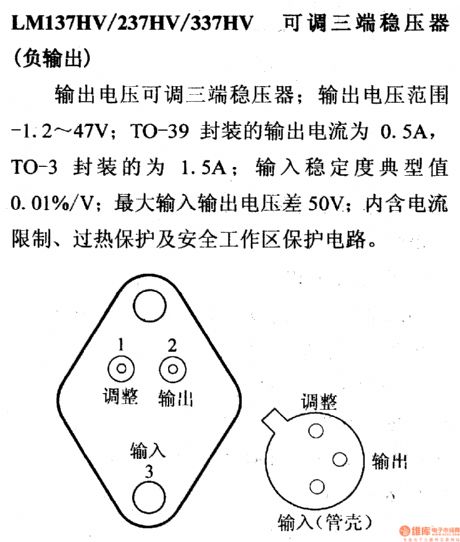
LM137HV/237HV/337HV--the adjustable 3-terminal stabilizer (negative output)This is an adjustable 3-terminal stabilizer; its output voltage range is -1.2~47V; the output current of the stabilizer in TO-39 package is 0.5A and TO-3 is 1.5A; the input stability typical value is 0.01%/V; the max input-output voltage difference is 50V; it contains the over-current limitation, over-heat protection and secure working area protection circuit.
(View)
View full Circuit Diagram | Comments | Reading(663)
The regulator: DC-DC circuit, power supply monitor pin and its main features LM136-5.0
Published:2011/8/30 0:38:00 Author:Seven | Keyword: DC-DC circuit, power supply, monitor pin
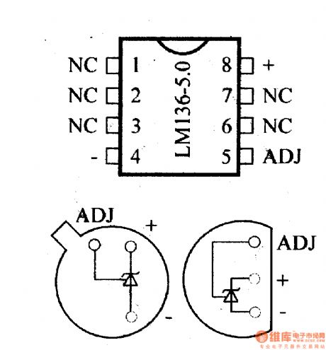
LM136-5.0/LM236-5.0/LM336-5.0--the Vref circuit (+5V)This is a high-precision and low-temperature drift Vref circuit; it works in the method of distributor; the output voltage is +5V; the Vref and temperature can be adjusted; the working current range is 0.4~10mA; the max reversed current is 15mA; the max forward current is 10mA; the working temperature of LM136-5.0 is -55~+125℃, LM236-5.0 is -25~+85℃ and LM336-5.0 is 0~70℃; LM136-2.5/LM236-2.5 is in metal package, LM336-2.5 is in metal or micro package and LM336-5.0 is in metal, plastic or micro package.
(View)
View full Circuit Diagram | Comments | Reading(986)
The regulator: DC-DC circuit, power supply monitor pin and its main features LM136-2.5/236-2.5/336-2.5
Published:2011/8/30 0:30:00 Author:Seven | Keyword: DC-DC circuit, power supply, monitor pin
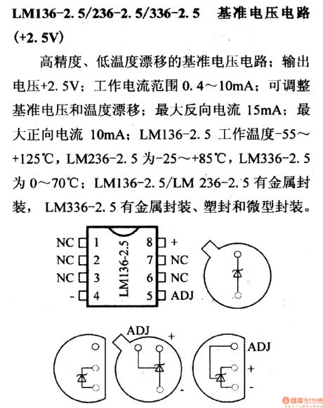
LM136-2.5/236-2.5/336-2.5--the Vref circuit (+2.5V)This is a high-precision and low-temperature drift Vref circuit; the output voltage is +2.5V; the working current range is 0.4~10mA; the Vref and temperature can be adjusted; the max reversed current is 15mA; the max forward current is 10mA; the working temperature of LM136-2.5 is -55~+125℃, LM236-2.5 is -25~+85℃ and LM336-2.5 is 0~70℃; LM136-2.5/LM236-2.5 is in metal package, LM336-2.5 is in metal, plastic or micro package.
(View)
View full Circuit Diagram | Comments | Reading(724)
3dd13 regulator constant current source circuit
Published:2011/9/4 20:30:00 Author:TaoXi | Keyword: regulator, constant current, source circuit
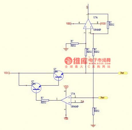
This is the numerical control constant current source that can be used to charge the storage battery. The D/A converter outputs a voltage value to the in-phase port of the op amp, the two ports of the current I=Uad/sampling resistor are used to connected with the + and - poles of the storage battery. The overhead op amp is connected into the amplifier circuit with the magnification of 1/4. This device is used to measure the voltage of the storage battery. The regulator 3dd13 is as shown in the figure. (View)
View full Circuit Diagram | Comments | Reading(1191)
3dd15 regulator constant current source circuit
Published:2011/9/4 20:27:00 Author:TaoXi | Keyword: regulator, constant current, source circuit
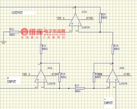
This is the numerical control constant current source that can be used to charge the storage battery. The D/A converter outputs a voltage value to the in-phase port of the op amp, the two ports of the current I=Uad/sampling resistor are used to connected with the + and - poles of the storage battery. The overhead op amp is connected into the amplifier circuit with the magnification of 1/4. This device is used to measure the voltage of the storage battery. The regulator 3dd15 is as shown in the figure.
(View)
View full Circuit Diagram | Comments | Reading(1709)
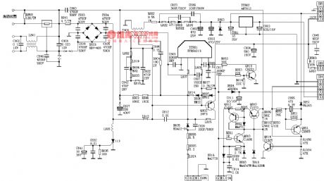
Panasonic M12H power supply circuit
Published:2011/9/4 19:56:00 Author:TaoXi | Keyword: Panasonic, power supply circuit
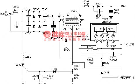
Oscilation circuit
The 300V DC voltage of the C836 adds to the C pole of the internal switching tube of the IC801's pin-1 through the primary windings P1 and P2 of the T801, and it adds to the B pole of the internal switching tube of the IC801's pin-2 through the R803, so the switching tube conducts. The current of E pole flows out from the pin-4 of IC801. The P1 and P2 winding current of T801 increases to produce the induced voltage, and this voltage is coupled with the F2 and F3 windings, the F2 has the positive induced voltage polarity, the F3 has the negative induced voltage polarity. This voltage adds to the pin-2 and pin-4 of the IC801 through the C806 and R804, so the switching current further increases, the strong positive feedback makes the switching tube saturated quickly.
(View)
View full Circuit Diagram | Comments | Reading(1267)
Hitachi NP8C power supply circuit
Published:2011/8/31 20:54:00 Author:TaoXi | Keyword: Hitachi, power supply circuit
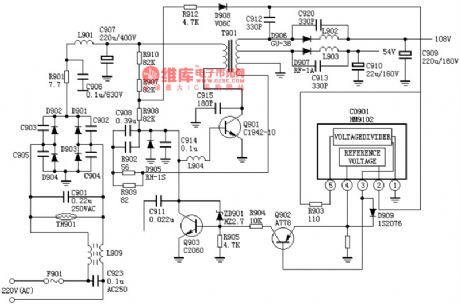
Oscillation process
The 300V DC voltage adds to the B pole of the switch tube Q901 through the R911, R907, R908, so the Q901 starts to conduct, the current flows through the primary winding of the T901, the Q901 produces the induced voltage, also the primary winding produces the induced voltage too. The voltage adds to the B pole of Q901 through the R902, R909, C908 to make the further conduction of Q901, the strong positive feedback makes the Q901 saturate rapidly.
In the saturated period of Q901, the D906 and D907 conduct, the T901 stores the energy, at the same time the positive feedback voltage charges the C908, so the voltage of the Q901's B pole is declining until the voltage can not maintain the saturation of Q901.
(View)
View full Circuit Diagram | Comments | Reading(1082)
Panasonic L15 power supply circuit
Published:2011/9/4 19:48:00 Author:TaoXi | Keyword: Panasonic, power supply circuit
Oscilation circuit
The 300V DC voltage of the C847 adds to the C pole of the internal switching tube of the IC801's pin-3 through the primary windings P1 and P2 of the energy storage transformer, and it adds to the B pole of the internal switching tube of the IC802's pin-2 through the R803, so the switching tube conducts. The winding voltage of P1 and P2 is coupled to the F2 and F3 windings to produce the positive feedback voltage, this voltage adds to the pin-2 and pin-4 of the IC801 through the C806 and R804, so the switching tube saturates rapidly.
During the switch saturation period, the current flows out from the pin-4 of the IC801 and builds the 113V DC voltage on C808.
(View)
View full Circuit Diagram | Comments | Reading(1392)
Sanyo 83P power supply circuit
Published:2011/8/31 22:05:00 Author:TaoXi | Keyword: Sanyo, 83P, power supply circuit
Oscillation process:
The 300V voltage of the positive port of C310 adds to the B pole of the switch tube BG311 through the R311 and R312, at the same time the No.4 and No.6 windings of the switching transformer B301 add to the C pole of BG311, the switch tube starts to conduct, the No.2 and No.3 windings of B301 produce the positive feedback voltage of No.2 positive and No.3 negative, this positive feedback voltage adds to the B pole of BG311 through the R335, D335, C333, the BG311 saturates rapidly.
After the BG311 is saturated, the current of the No.4 and No.6 windings of B301 increases linearly, the B301 stores the magnetic energy. The E pole current of BG311 gets through the R330 and produces the linear-increasing sawtooth voltage on R330.
(View)
View full Circuit Diagram | Comments | Reading(1087)
SANYO 80P power supply circuit
Published:2011/8/31 21:54:00 Author:TaoXi | Keyword: SANYO, 80P, power supply circuit
Oscillation process
The 300V DC voltage adds to the B pole of the switch tube Q504 through the R518, R519, the Q504 starts to conducts. The pin-9 and pin-10 of the T501 are the positive feedback winding, the pin-9 has the positive polarity and the pin-10 has the negative positive polarity, the voltage gets through the positive feedback which is composed of the B, E poles of Q504, the R516, R515 and D509 to make the Q504 saturate rapidly.
After the Q504 is saturated, the primary winding current of T501 increases linearly, this current produces the sawtooth wave voltage-drop on the R514, the voltage-drop adds to the B pole of Q502 through the R505 and C507, the sawtooth wave voltage is superimposed on the 6.8V DC voltage of the B pole of the Q502, when the B pole voltage of Q502 is lower than a set value, the Q502 conducts to make the left port of C510 connect with the ground.
(View)
View full Circuit Diagram | Comments | Reading(1385)
Hitachi NP84C power supply circuit
Published:2011/8/31 21:08:00 Author:TaoXi | Keyword: Hitachi, power supply circuit

Oscillation process
The 300V DC voltage adds to the B pole of the switch tube Q901 through the R902, R903, C905, so the Q901 starts to conduct, the current of the C pole flows through the pin-1 and pin-3 of the primary winding of the T901, the Q901 produces the induced voltage, also the pin-5 and pin-10 of the primary winding produces the induced voltage too. The voltage adds to the B pole of Q901 through the R905, C911, R906, C908 to make the further conduction of Q901, the strong positive feedback makes the Q901 saturate rapidly.
In the saturated period of Q901, the winding current of the T901's pin-1 and pin-3 increases to build the 110 V DC voltage on C909. At the same time, in the saturated period of Q901, the C911 is charged constantly to make the B pole voltage of Q901 become smaller, at last the Q901 exits the saturated state.
(View)
View full Circuit Diagram | Comments | Reading(1121)
Sun Battery Charger Circuit
Published:2011/7/23 6:47:00 Author:Michel | Keyword: Sun Battery, Charger Circuit
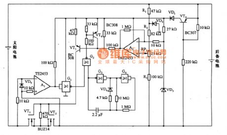
The above picture is sun battery charger circuit.Electronic filter (VT5) and regulating diode,VD3 constitute regulating circuit.Its stable voltage is used as benchmark voltage of A2 reverse phase input terminal.Measuring battery voltage of resistance R1,R2,R3 and RP1 are added to A2 phase input terminal. When it is lower than benchmark voltage,A2 outputs low PWL,VT3,VT1 and VT2 conduct.If the sun battery voltage is higher than the backup battery voltage,it begins to charge the backup voltage.A1 test sun battery voltage is lower thsn backup battery voltage,A1 outputs low PWL.G3 and G4 are harmonic oscillators and it produces 15 ms pulse every 15s.A1 compares backup battery voltage and the sun battery voltage,for example,VT1 and VT2 is still in cut-off condition if sun battery is lower than backup battery. (View)
View full Circuit Diagram | Comments | Reading(1899)
The switch power supply of STR5412
Published:2011/8/13 2:25:00 Author:qqtang | Keyword: switch power supply
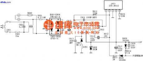
View full Circuit Diagram | Comments | Reading(2290)
C6458 power supply circuit
Published:2011/8/26 3:32:00 Author:TaoXi | Keyword: power supply
View full Circuit Diagram | Comments | Reading(1038)
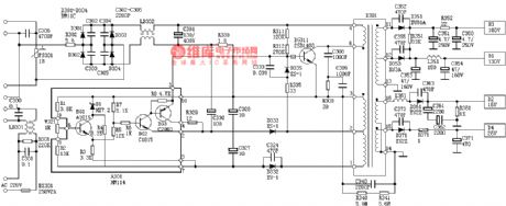
Hitachi A1PM8C power supply circuit
Published:2011/8/29 2:42:00 Author:TaoXi | Keyword: Hitachi, power supply
The oscillation process
The 220V AC voltage is fully rectified by the circuit to produce the 300V DC voltage on C906, and this DC voltage adds to the pin-3 of the IC901 through the L1 winding resistor of T901, at the same time the 220V voltage is half-wave rectified by the circuit and the voltage adds to pin-2 of IC901 through the R942, R903, R904, the internal switching tube of IC901 conducts, the current of L1 of the T901 increases, the winding resistor L2 produces the positive feedback voltage, this voltage adds to the pin-2 of the IC901 through the Q901, D905, L907, so the internal switch tube of IC901 saturates quickly.
During the switch turn-on period, the winding resistor L2 charges the C905 through the R906 and R907, and it charges the C909 through the R909, the charging result of the C909 is the electric potential decreasing of the pin-1 of IC901.
(View)
View full Circuit Diagram | Comments | Reading(1843)
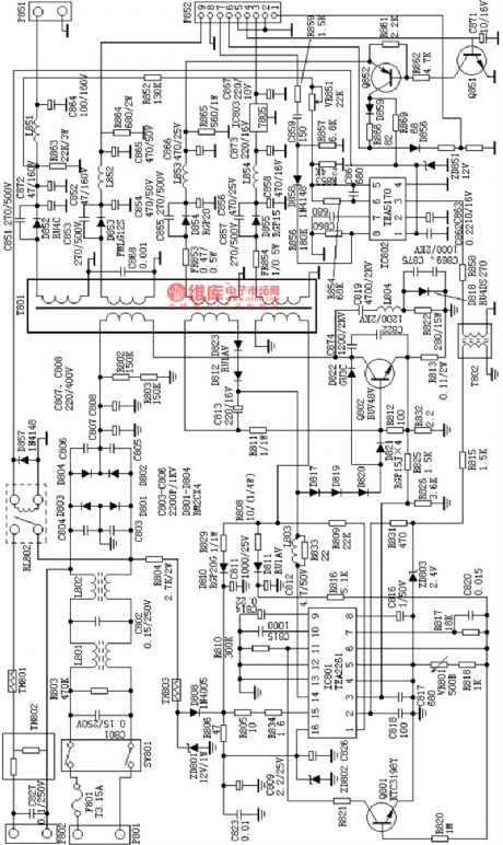
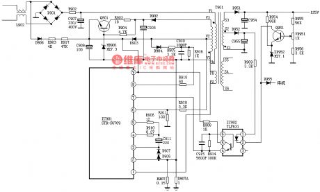
Hitachi A3P-B2 power supply circuit
Published:2011/8/29 3:29:00 Author:TaoXi | Keyword: Hitachi, power supply
Oscillation process
If you add the voltage which is more than 6V to the pin-9 of STR6709, the switch power supply will start oscillating.
The voltage of C907 is about 300V, it adds to the C electrode of the IC901's pin-1 internal switch tube through the P1 and P2 winding resistors, and the 220V AC is rectified by D908, then it is limited by R903 and R917 and filted by C909 to be the unstable DC voltage, this DC voltage adds to the pin-9 of IC901, the switch power supply starts oscillating. After the power supply is started, the induced voltage of V1 and V2 are rectified by D903 to be the 9.5V voltage, and it supplies the power to pin-9 of IC901. Q901 is intended for the power supply of IC901's pin-9 in the standby state.
(View)
View full Circuit Diagram | Comments | Reading(2500)
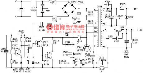
+5V input +30V output boost circuit
Published:2011/8/29 3:48:00 Author:TaoXi | Keyword: +5V, input, +30V, output, boost circuit
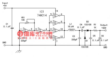
The +5V input +30V output boost circuit
(View)
View full Circuit Diagram | Comments | Reading(1142)
| Pages:62/291 At 206162636465666768697071727374757677787980Under 20 |
Circuit Categories
power supply circuit
Amplifier Circuit
Basic Circuit
LED and Light Circuit
Sensor Circuit
Signal Processing
Electrical Equipment Circuit
Control Circuit
Remote Control Circuit
A/D-D/A Converter Circuit
Audio Circuit
Measuring and Test Circuit
Communication Circuit
Computer-Related Circuit
555 Circuit
Automotive Circuit
Repairing Circuit