
power supply circuit
Index 73
10000_V_WITH_ZENER
Published:2009/7/15 22:17:00 Author:Jessie
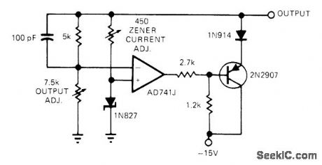
Circuit provides stable current biasing of zener and adjustable output voltage by bootstrapping excitation current off output voltage. Commercial version of circuit (Analog Devices AD2700) achieves temperature drift of only 3 PPM/℃.-J. Williams, Don't Bypass the Voltage Reference That Best Suits Your Needs, EDN Magazine, 0ct. 5, 1977, p 53-57. (View)
View full Circuit Diagram | Comments | Reading(862)
AUDIO_CONTROLLED_LAMP_DIMMER
Published:2009/7/15 22:17:00 Author:Jessie
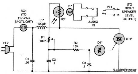
The audio input to J1 lights low-voltage lamp I1. This light illuminates light-dependent resistor R3 (100 KΩ to 1 MΩ dark resistance) and modulates the intensity of the lamp plugged into SO1. L1 and C1 suppress RFI caused by the triac phase-control circuit. D1 and TR1 are a diac and a triac, respectively, and are the types used in common lamp dimmers. (View)
View full Circuit Diagram | Comments | Reading(1169)
5_V_FROM_15_V
Published:2009/7/15 22:16:00 Author:Jessie
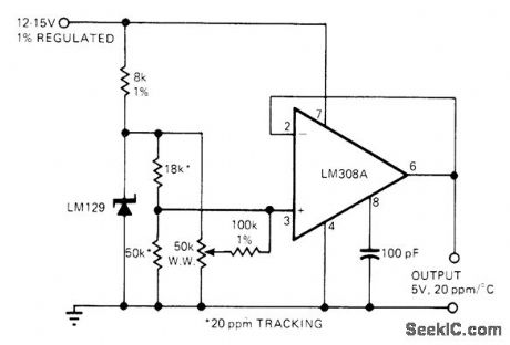
Used as reference for A/D converter when reference voltage required is below that of zener, permitting simplified circuit design. Zener drift contributes proportionally to output temperature drift, while opamp offset drift contributes at greater rate. Opamp is unnecessary if high output impedance can be tolerated.-R. C. Dobkin, Don't Forget Reference Stability When Designing A-to-D Converters, EDN Magazine, June 20, 1977, p 105-108. (View)
View full Circuit Diagram | Comments | Reading(835)
DELAYED_PULSE
Published:2009/7/15 22:15:00 Author:Jessie
Both time and duration of output pulse are programmable by selection of RC networks. Original and delayed clock pulses can both be used in gating circuits. With values shown, output pulse is 1 ms wide and is delayed 15 μs from trailing edge of clock pulse.-D. T. Anderson, Operational Amplifier Makes a Simple Delayed Pulse Generator, EDN Magazine, July 1, 1972, p 55. (View)
View full Circuit Diagram | Comments | Reading(826)
_15_V_HIGH_PRECISION
Published:2009/7/15 22:15:00 Author:Jessie

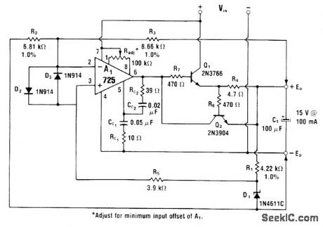
Uses 725 opamp having low offset drift and high common-mode rejection in combination with low-drift version of 1N4611 zener to give highly stable operation at output currents up to 100 mA. Close-tolerance low-temperature-coefficient film or wirewound resistors are required for R1, R2, and R3. Remote sensing at load corrects for wiring voltage drops.-W. G. Jung, IC Op-Amp Cookbook, Howard W. Sams, Indianapolis, IN, 1974, p 152-155. (View)
View full Circuit Diagram | Comments | Reading(739)
PREFERRED_MONOSTABLE
Published:2009/7/15 22:12:00 Author:Jessie

Generates positive or negative rectangular gate in response to positive input trigger. Duration of gate will remain within 5% of initial preset value, and amplitude will be constant within 30%. Circuit is self-timing, with output gate duration determined by configuration and values of R3, R4, and C3. Used in radar to establish period during which main display sweep is presented, to provide crt unblanking gate, and to provide enabling gate for distance mark generator.-NBS, Handbook Preferred Circuits Navy Aeronautical Electronic Equipment, Vol. I, Electron Tube Circuits, 1963, PC 41, p 41-2. (View)
View full Circuit Diagram | Comments | Reading(834)
101_V_STANDARD_CELL_REPLACEMENT
Published:2009/7/15 22:11:00 Author:Jessie
National LM199 temperature-stabilized 6.95-V reference is applied to LM3308 opamp through LM321 preamp to give standard-cell replacement that can be adjusted to output of exactly 1.01 V. Null offset of opamp before adjusting for proper output voltage, - Linear Applications, vol. 2, National Semiconductor, Santa Clara, CA, 1976, AN-161, p 5. (View)
View full Circuit Diagram | Comments | Reading(880)
±25_V
Published:2009/7/15 22:11:00 Author:Jessie
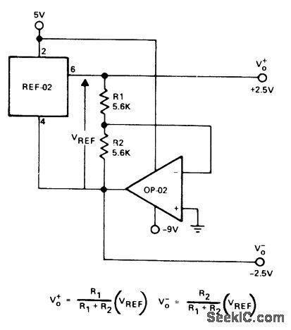
Precision Monolhhics REF-02 voltage reference and OP-02 inverting opamp provide desired references when used with supply volt-ages shown.- +5 V Precision Voltage Reference/Thermometer, Precision Monolithics, Santa Clara, CA, 1978, REF-02, p 6. (View)
View full Circuit Diagram | Comments | Reading(857)
10_V_WITH_MODERATE_DRIFT
Published:2009/7/15 22:10:00 Author:Jessie

Suitable for A/D converter applications in which output voltage can drift as much as 20 PPM/℃. Temperature-drift error is divided equally between zener and amplifier, permitting use of moderately low-drift components.-R. C. Dobkin, Don't Forget Reference Stability When Designing A-to-D Converters, EDN Magazine, June 20, 1977, p 105-108. (View)
View full Circuit Diagram | Comments | Reading(840)
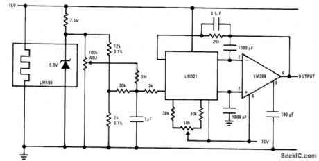
10_V_WITH_TC_TRIMMlNG
Published:2009/7/15 22:09:00 Author:Jessie
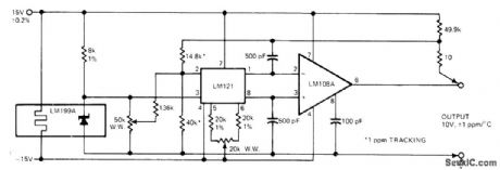
Provides temperature-compensation trimming to give lowest possible reference-voltage drift for A/D converter. Reference zener is LM199A having 0.5 PPM/℃ drift that is independent of operating current. Low-drift combination of LM121 and LMl08A has drift predictably proportional to offset voltage, permitting use of potentiometers for trimming to better than 1 PPM/℃. Article gives details of trimming procedure to be used during temperature runs.- R. C. Dobkin, Don’t Forget Reference Stabillity When Desiging A-to-D Converters, EDN Magazine, June 20, 1977, p l05-108. (View)
View full Circuit Diagram | Comments | Reading(891)
65_V_REFERENCE
Published:2009/7/15 22:07:00 Author:Jessie
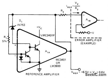
Reference amplifier uses mirror characteristic of noninverting input of current-mode opamp to determine zener current. Resulting voltage drop across zener provides, through R2, current reference for other or opamps or compensated voltage reference.-R. W Fergus, Use Current-Mode Op Amps in Reference Circuits, EDN Magazine, June 20, 1974, p 80 and 83. (View)
View full Circuit Diagram | Comments | Reading(849)
LOW_DRIFT_MICROPOWER
Published:2009/7/15 22:05:00 Author:Jessie
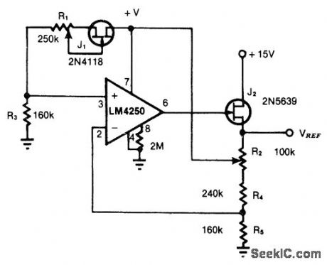
Uses JFET biased slightly below pinchoff in combination with micropower opamp to convert zero-temperature-coefficient drain current to correspondingly stable reference voltage. Additional JFET J2 makes operation independent of value of unregulated input. Output impedance is low. For higher output impedance, reference voltage can be taken from wiper of R2, but buffering could then be required. R1, is adjusted to compensate for temperature coefficient arising from opamp supply current.-N. Sevastopoulos and J. Mayer, Micropower Reference Stays Stable, EDN Magazine, Sept. 5, 1978, p 158. (View)
View full Circuit Diagram | Comments | Reading(1030)
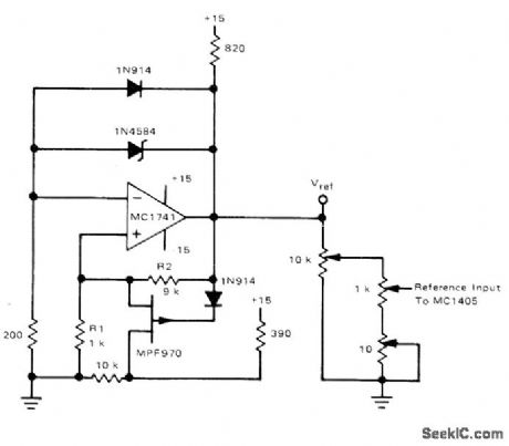
_66_V_WITH_741_OPAMP
Published:2009/7/15 22:04:00 Author:Jessie
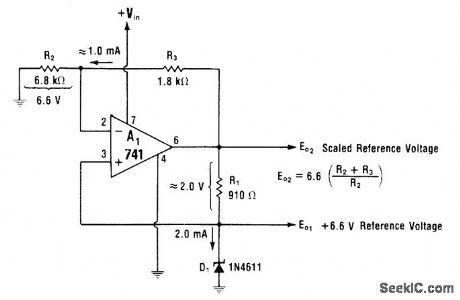
Uses combination of negative and positive feedback to maintain constant current of 2 mA in D1, independent of variations in ambient temperature and unregulated input. Reference voltage of 6.6V, determined by breakdown voltage of 1N4611 zener, is scaled up to more positive level at output of A1. Scaled output has low impedance and can supply appreciable current without affecting reference voltage accuracy. Supply must be single-ended for reliable starting.-W. G. Jung, IC 0p-Amp Cookbook, Howard W. Sams, Indianapolis, IN, 1974, p 141-143. (View)
View full Circuit Diagram | Comments | Reading(0)
FET_LINEAR_MODULATOR
Published:2009/7/15 21:49:00 Author:Jessie
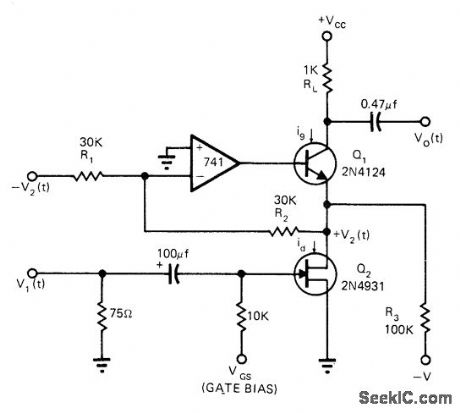

Circuit developed for closed.-circuit industrial color television system uses linear portion of operating characteristic for 2N4931 FET to provide linear response at modulation frequencies from 1 MHz down to near zero. Article gives design equations.-G.R. Shapiro, Analog Multipliers Offer Solutions to Video Modulation Problems, EDN Magazine Sept 1,1972, p 40-41. (View)
View full Circuit Diagram | Comments | Reading(917)
CHARACTER_FORMING_DOT_GENERATOR
Published:2009/7/15 21:49:00 Author:Jessie
Transistor switch, having drop of less than 50 mv when delivering 50 ma, is used in display that provides fast alphanumeric readout on crl by forming characters from series of overlapping dots.-S. C. Chao, Character Displays Using Analog Techniques, Electronics, 32:43, p 116-118. (View)
View full Circuit Diagram | Comments | Reading(861)
NANOSECOND_PULSE_DISPLAY
Published:2009/7/15 21:48:00 Author:Jessie
Magnetic-focus electrostatic-deflection beam-deflection tube permits pulse height analysis where pulse separation is of the order of microseconds.-J. Burns, Special Tubes for Nanosecond Display, Electronics, 33:49, p 82-85. (View)
View full Circuit Diagram | Comments | Reading(771)
SINGLE_PULSE_SELECTOR
Published:2009/7/15 21:43:00 Author:Jessie
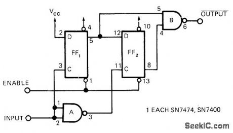
Circuit is used to select any desired single pulse from wavetrain continuously applied to input terminal. When enable pulse (not exceeding width of input pulse) is applied, flip-flop FF1 clocks on leading edge of next input pulse and FF2 clocks on trailing edge. Output pulse thus has same width as pulses in input wavetrain. Edge-triggering characteristics of D flip-flops prevent operation if they are enabled during input pulse; in this case, next input pulse is delivered as output.-S. J. Cormack, Pulse Catcher Uses Two ICs, EDN Magazine, Jan. 5, 1973, p 109. (View)
View full Circuit Diagram | Comments | Reading(1028)
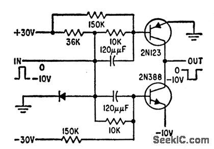
1_V_HIGH_PRECISION
Published:2009/7/15 21:36:00 Author:Jessie
Drift is less than 1 mV over 20℃ temperature range, and voltage dividet reduces this to ±0.1 mV for 1.00-V reference required in 41/2 -digit meter. All three pots should be wirewound. Current of reference zener is regulated by opamp gain and zener voltage.-S. Kelley, Applications of MC1405/MC14435 in Digital Meters, Motorola, Phoenix, AZ, 1975, AN-748, p 19. (View)
View full Circuit Diagram | Comments | Reading(1047)
10_MC_TD_MVBR
Published:2009/7/15 23:19:00 Author:Jessie
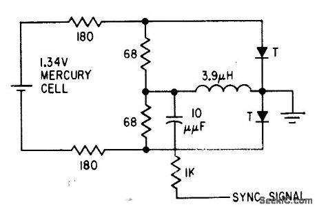
Uses two 1-ma, 0.01-ohm tunnel diodes.-I. A, Lesk, N. Holonyak, Jr., and U. S. Davidsohn, The Tunnel Diode-Circuits and Applications, Electronics, 32:48, p 60-64. (View)
View full Circuit Diagram | Comments | Reading(869)
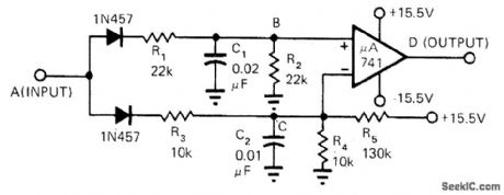
SUPPRESSING_NOISES_UP_TO_1000_TIMES_SIGNAL_LEVEL
Published:2009/7/15 23:18:00 Author:Jessie
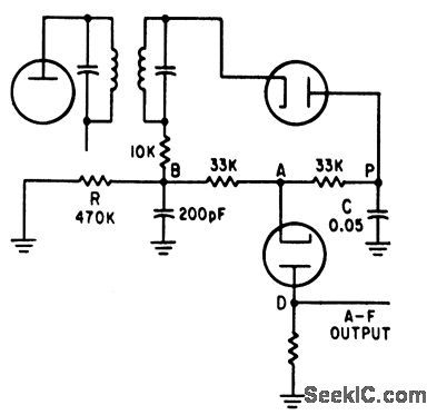
Improved noise limiter for airborne transceiver uses large RC time constant. Plate of detecting diode is negatively charged by a-f signal, held steady by C. For noise impulses, point A swings positively and limiter diode blocks rectified noise signal.-K. Makino and T. Yamanaka, Servo-Tuned Transceiver for Airborne VHF Communications, Electronics, 35:1, p 82-85 (View)
View full Circuit Diagram | Comments | Reading(774)
| Pages:73/291 At 206162636465666768697071727374757677787980Under 20 |
Circuit Categories
power supply circuit
Amplifier Circuit
Basic Circuit
LED and Light Circuit
Sensor Circuit
Signal Processing
Electrical Equipment Circuit
Control Circuit
Remote Control Circuit
A/D-D/A Converter Circuit
Audio Circuit
Measuring and Test Circuit
Communication Circuit
Computer-Related Circuit
555 Circuit
Automotive Circuit
Repairing Circuit