
Circuit Diagram
Index 1016
DIGITAL_FOURIER
Published:2009/7/6 21:34:00 Author:May
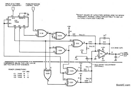
Sine-wave generator produces Walsh-function approximation of sine function. Frequency of sine wave is set by square-wave input to pin 14 of 7493. Filter com ponents of opamp help smooth staircase wave form generated by summing Walsh-function components as weighted by resistors. Circuit is converter consisting of digital expander that expands input square wave into variety of digital waveforms and analog combiner that adds these waveforms to produce periodic analog output. Negative signs of Walsh harmonics are handled with digital inverter, and magnitudes are handled by choice of resistor value in summing junction. Signs and magnitudes are under microprocessor control. Net output is stairstep approximation to desired output, which can be smoothed by low-pass filter.-B. F. Jacoby, Walsh Functions: A Digital Fourier Series, BYTE, Sept. 1977, p 190-198. (View)
View full Circuit Diagram | Comments | Reading(2648)
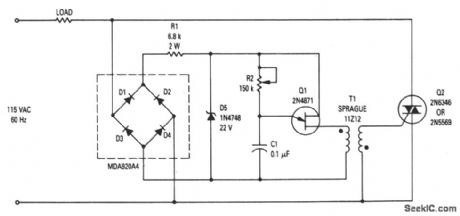
POLICE_ALERTING_ALARM
Published:2009/7/22 0:03:00 Author:Jessie
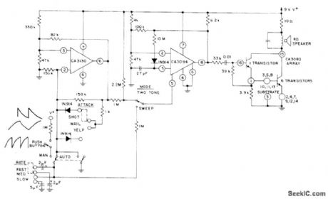
Combination of CA3130 bipolar MOS opamp, CA3094 programmable opamp, and CA3082 transistor array develops large signal swings with various waveforms required for driving loudspeakers to produce attention-getting siren and other sounds. CA3094 is connected as VCO for generating tones that are combined with output of CA3130 astable MVBR to develop required signal swings.- Circuit Ideas for RCA Linear ICs, RCA Solid State Division, Somerville, NJ, 1977, p8. (View)
View full Circuit Diagram | Comments | Reading(990)
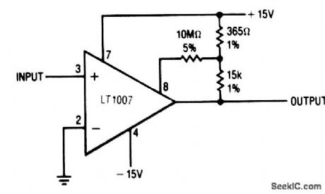
PRECISION_COMPARATOR_WITH_BALANCED_INPUTS_AND_VARIABLE_OFFSET
Published:2009/7/6 21:33:00 Author:May
View full Circuit Diagram | Comments | Reading(749)
CALIBRATING_MARK_SPACE_VCO
Published:2009/7/6 21:32:00 Author:May
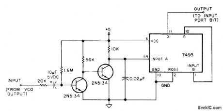
Simple buffer/counter provides accurate calibration of FSK circuit used in cassette interface of 8080 microprocessor to generate mark and space frequencies. Audio FSK waveform is squared and divided down in 7493 4-bit counter. Resulting pulses are fed to input port of microprocessor for software pulse counting. Software sets VCO frequency, waits until pulse starts, counts each pulse occurrence, and displays resultant count.Each 7493 count is 29 Hz or 14.5μs, so 371 counts correspond to 2975 Hz for space. Mark frequency of 2125 Hz gives pulses separated by 519 counts.-D. R. Bourdeau, Cassette Interface First Aid, Kilobaud, July 1977, p 49. (View)
View full Circuit Diagram | Comments | Reading(1594)
FREQUENCY_DETECTING_COMPARATOR
Published:2009/7/6 21:30:00 Author:May
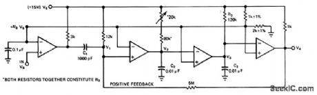
A quad comparator forms the basis of a frequency detector that is faster and less expensive than more complex versions designed around frequency-to-voltage converter chips. Positive feedback through a 5-MΩ resistor allows the circuit to resolve changes as small as two percent; the output responds to those changes in about one cycle. When the input frequency is high, V2 is pulled low; it's never allowed to exceed 2/3 V. When the input frequency is lower than the limit, V2 exceeds 2/3 V once each cycle, but V3 is held below that limit. The trip frequency is defined by F = 1/(1.1R2C2). R2 can be adjusted to permit trimming of the trip point, but the value of R3 must remain larger than R2. (View)
View full Circuit Diagram | Comments | Reading(843)
VARIABLE_SQUARE_TRIANGLE_
Published:2009/7/6 21:30:00 Author:May
Dual pot R1-R3 varies frequency over range of 15-500 Hz when C1 is in circuit and 150-4800 Hz when C2 is in circuit. Each output has amplitude control.Opamps are Motorola MC3401P or National LM3900, and transistors are 2N2924 or equivalent NPN. Supply can be 12 VDC.-C. D. Rakes, Integrated Circuit Projects, Howard W. Sams, Indianapolis, IN, 1975, p 19-20. (View)
View full Circuit Diagram | Comments | Reading(677)
12_BITS_ON_8_BIT_BUS
Published:2009/7/6 21:28:00 Author:May
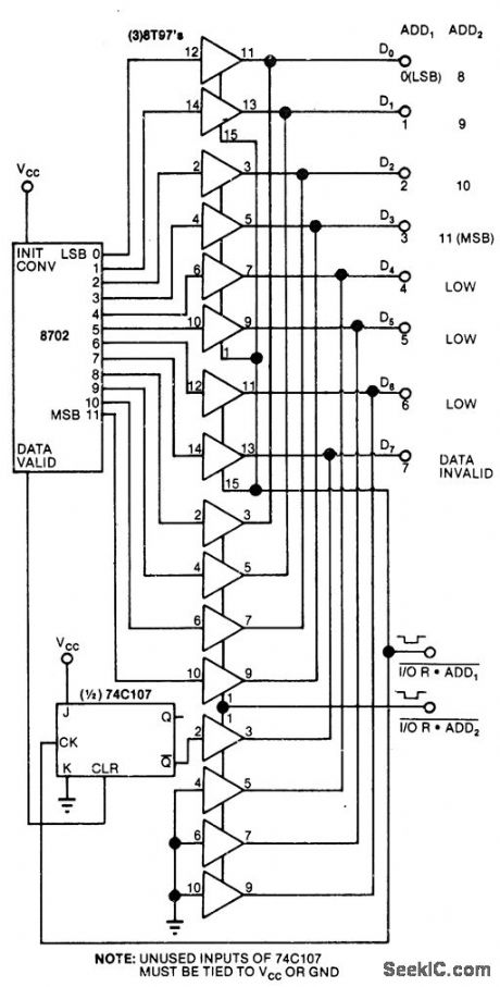
Arrangement shown speeds reading of 12 bits of data onto 8-bit microprocessor bus by simplifying checking procedure. Output of 74C107 flip-flop becomes DATA INVALID bit and is placed on bus during second read cycle. Simultaneously, circuit pulls 3 remaining bits (D4-D6) low through use of spare 8T97 gates. Article gives simplified 8080 subroutine required.-D. W. Taylor, Speed-Read 12 Bits onto an 8-Bit Bus, EDN Magazine, Sept. 5, 1978, p 70. (View)
View full Circuit Diagram | Comments | Reading(768)
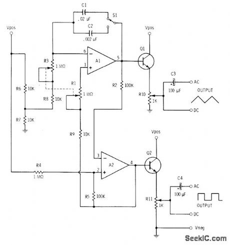
COMPARATOR_LATCH
Published:2009/7/6 21:27:00 Author:May
The primary advantage of this circuit, when compared to other comparators, is its ability to latch after the input has reached a predetermined threshold level. When the input exceeds the threshold level, the LM311N output increases.This transition enables the strobe input, preventing the output from falling low. A high-level voltage on the reset input will turn off Q1, thereby removing the supply voltage from the open collector output of the LM311N. With no supply to the strobe input, the latch condition is removed and the output is again allowed to follow the input excursions. The LM311N will operate with a wide variety of supply voltage levels, ranging from dual ±15 V to a single 5 V level that provides compatibility with digital IC logic. If more than one latch is used with a common reset, all the pull-up resistors may be connected to Q1's collector. (View)
View full Circuit Diagram | Comments | Reading(2853)
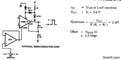
MICROVOLT_COMPARATOR_WITH_HYSTERESIS
Published:2009/7/6 21:26:00 Author:May
Positive feedback to one of the nulling terminals creates approximately 5 μV of hysteresis. The output can sink 16 mA; the input offset voltage is typically changed less than 5μV because of the feedback. (View)
View full Circuit Diagram | Comments | Reading(840)
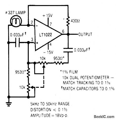
AUDIO_OSCILLATOR
Published:2009/7/6 21:26:00 Author:May
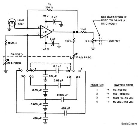
Circuit Notes
A Wien bridge oscillator produces sine waves with very low distortion level. The Wien bridge oscillator produces zero phase shift at only one frequency (f=1/2π RC) which will be the oscillation frequency. Stable oscillation can occur only if the loop gain remains at unity at the oscillation frequency. The circuit achieves this control by using the positive temperature coefficient of a small lamp to regulate gain (Rf/RLAMP) as the oscillator attempts to vary its output. The oscillator shown here has four frequency bands covering about 15 Hz to 150 kHz. The frequency is continuously variable within each frequency range with ganged 20 k ohm potentiometers. The oscillator draws only about 4.0 mA from the 9-V batteries. Its output is from 4 to 5 V with a 10 k ohm load and the Rf (feedback resistor) is set at about 5% below the point of clipping. As shown, the center arm of the 5 k ohm output potentiometer is the output terminal. To couple the oscillator to a dc type circuit, a capacitor should be inserted in series with the output lead. (View)
View full Circuit Diagram | Comments | Reading(0)
WINDOW_COMPARATOR
Published:2009/7/6 21:25:00 Author:May
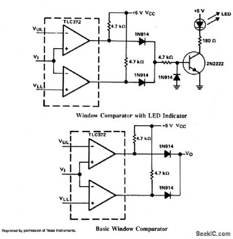
A window detector is a specialized comparator circuit designed to detect the presence of a voltage between two prescribed limits; that is, within a voltage window. This circuit is implemented by logically combining the outputs of two single-ended comparators by the IN914 diodes. When the input voltage is between the upper limit, VUL, and the lower limit, VLL, the output voltage is zero; otherwise it equals a logic high level. The output of this circuit can be used to drive a logic gate, LED driver, or relay driver circuit. The circuit shown in Fig. 16-1 shows a 2N2222 npn transistor being driven by the window comparator. When the input voltage to the window comparator is outside the range set by the VUL and VLL inputs, the output changes to positive, which turns on the transistor and lights the LED indicator.
(View)
View full Circuit Diagram | Comments | Reading(0)
Strain_gauge_with_thermoelectric_junction_effects
Published:2009/7/22 3:41:00 Author:Jessie
This circuit shows the previous strain-gauge example (Fig. 1-11) with low-level nodes highlighted and shown as thermoelectric junctions. An even number of connections cancels the errors as long as no temperature gradients appear across the circuit. Such gradients are best prevented by symmetric PC layouts with traces sized for matched thermal conductivity. In extreme cases, the circuitry can also be insulated from external heat sources and drafts. (View)
View full Circuit Diagram | Comments | Reading(929)
PARALLEL_TO_SERIAL__CONVERTER
Published:2009/7/6 21:24:00 Author:May
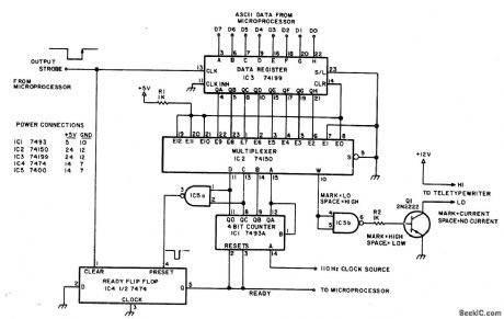
Multiplexer IC2 selects formatting and data bits according to state of IC1, IC3 is output latch Teletypewriter current loop is driven by Q1 from output of multiplexer. 110-Hz clock gives transfer rate of 10 characters per second. Provides standard asynchronous format of 1 start bit, 8 data bits, and 2 stop bits for teletypewriter without using universal asynchronous receiver-transmitter,-G. C. Jewell, How to Drive a Teletype Without a UART, BYTE, Jan, 1977, p 32. (View)
View full Circuit Diagram | Comments | Reading(2612)
LOW_DISTORTION_SINE_WAVE_OSCILLATOR
Published:2009/7/6 21:22:00 Author:May
View full Circuit Diagram | Comments | Reading(0)
SINE_WAVE_SHAPER
Published:2009/7/6 21:20:00 Author:May
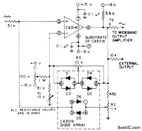
Circuit Notes
Uses a CA3140 BiMOS op amp as voltage follower, together with diodes from a CA3019 array, to convert a triangular signal (such as obtained from a function generator) to a sine-wave output with typical THD less than 2%. (View)
View full Circuit Diagram | Comments | Reading(2363)
NE602_VOLTAGE_TUNED_LOCAL_OSCILLATOR_CIRCUITS
Published:2009/7/22 3:39:00 Author:Jessie
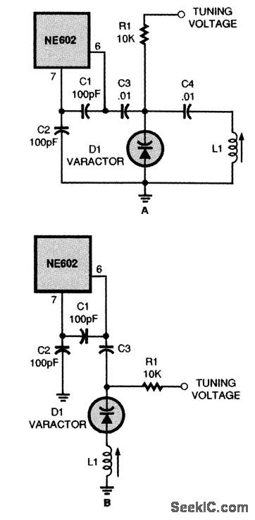
The LO circuit for the NE602 can also be voltage controlled. Here are two different voltage-tuned local-oscillator circuits. (View)
View full Circuit Diagram | Comments | Reading(705)
800_W_light_dimmer
Published:2009/7/22 3:38:00 Author:Jessie
This circuit shows the basic UJT building block (Fig. 9-1) that is used to control power applied to incandescent lights. R2 varies the time constant of the timing circuit, and thus provides phase control for the triac. Power to the lights is controlled by varying the conduction angle of the triac from 0° to 170°. The power available at the 170°-conduction angle is better than 97% of that at the 180° angle. (View)
View full Circuit Diagram | Comments | Reading(0)
8_BITS_CONTROL_128_BITS
Published:2009/7/6 21:20:00 Author:May
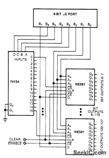
Combination of 74154 demultiplexer and 16 NE591 latches permits control of 128 single-bit outputs with standard 8-bit parallel output of microprocessor. Latches are driven from three low-order bits of microprocessor. Next four higher bits drive 74154 which in turn drives chip-enable inputs of NE591s. Eighth bit of microprocessor drives data inputs of all latches and sets addressed bits appropriately.-R. D. Grappel, Control 128 Bits with an 8-BitμC Port, EDN Magazine, Sept. 5, 1978, p 70 and 72. (View)
View full Circuit Diagram | Comments | Reading(1510)
SQUARE_TO_SINE_WITH_PLL
Published:2009/7/6 21:19:00 Author:May
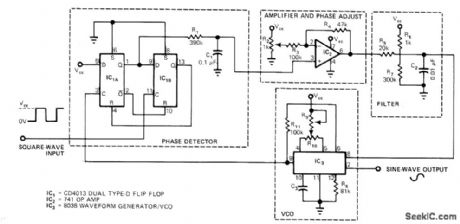
8038 Wavefrom generator simultaneously generates synthesized sine wave and square wave. Square-wave output closes phase-locked loop through 741 opamp IC2 and dual flip-flop IC1, while sine-wave output functions as converted output. Center frequency is 0.15/R9C3. R10 should be at least 10 times smaller than R9. If center frequency is 400 Hz, capture range is half that or ±100 Hz. When input is applied, phase comparator generates voltage related to frequency and phase difference of input and free-running signals, lC2 amplifies and offsets phase-difference signal. Sine output has less than 1% distortion, DC component of 0.5 Vcc, and minimum amplitude of 0.2 Vcc P-P.-L.S.Kasevich, PLL Converts Square Wave into Sine Wave, EDN Magazine, June 20, 1978, p 128. (View)
View full Circuit Diagram | Comments | Reading(2414)
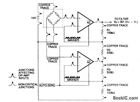
Strain_gauge_amplifier
Published:2009/7/22 3:37:00 Author:Jessie
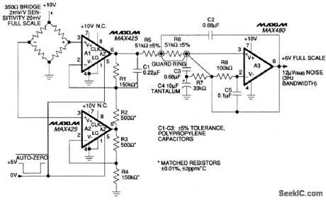
In the circuit, two MAX425s (A1 and A2) amplify the differential 20-mV full-scale output of a strain-gauge bridge. The signal is then filtered and buffered by a MAX480 (A3). The 3-Hz bandwidth of the filter limits output noise to about 12 μVrms (40 nVrms referred to the input). This translates to a signal-to-noise ratio of 114dB, which allows stable measurements to within a few parts per million. (View)
View full Circuit Diagram | Comments | Reading(3484)
| Pages:1016/2234 At 2010011002100310041005100610071008100910101011101210131014101510161017101810191020Under 20 |
Circuit Categories
power supply circuit
Amplifier Circuit
Basic Circuit
LED and Light Circuit
Sensor Circuit
Signal Processing
Electrical Equipment Circuit
Control Circuit
Remote Control Circuit
A/D-D/A Converter Circuit
Audio Circuit
Measuring and Test Circuit
Communication Circuit
Computer-Related Circuit
555 Circuit
Automotive Circuit
Repairing Circuit