
Circuit Diagram
Index 1012
FET_BALANCED_MODULATOR_FOR_SSB
Published:2009/7/6 22:58:00 Author:May
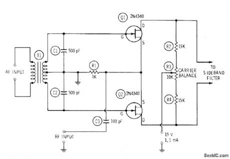
AF modulating signal is applied to gates of matched FETs in push-pull through T1 having accurately center-tapped secondary, and RF carrier is applied to sources in parallel through C3. Carrier is canceled in output circuit, leaving two sidebands. R3 is adjusted to correct for un-balance in circuit components.-R. P. Turner, FET Circuits, Howard W. Sams, Indianapolis, IN, 1977, 2nd Ed., p 90-91. (View)
View full Circuit Diagram | Comments | Reading(2471)
DUTY_CYCLE_MODULATOR
Published:2009/7/6 22:56:00 Author:May
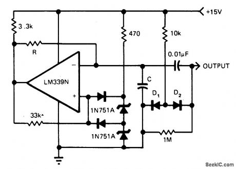
Uses half of LM339N or LM3302N quad comparator. With no modulation signal, output is symmetrical square wave generated by one of comparators. Constant-amplitude triangle wave is generated at inverting input of second comparator, and is relatively independent of supply voltage and frequency changes. Modulating signal varies switching points to produce duty-cycle modulated wave for such applications as class D amplification for servo and audio systems.-H. F. Stearns, Voltage Comparator Makes a Duty-Cycle Modulator, EDN Magazine, June 5, 1975, p76-77. (View)
View full Circuit Diagram | Comments | Reading(1202)
BALANCED_MODULATOR
Published:2009/7/6 22:51:00 Author:May
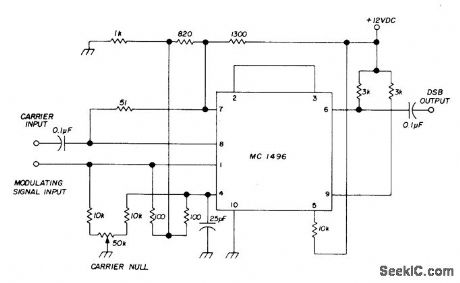
High-performance balanced modulator for 80-meter SSB transceiver uses Motorola MC1496IC,Adjust 50K pot for maximum carrier suppression of doublesideband output.-D, Hembling, Solid-State 80-Meter SSB Transceiver, Ham Radio, March1973,p6-17 (View)
View full Circuit Diagram | Comments | Reading(5278)
TRIANGLE_WAVE_CLIPPER
Published:2009/7/6 22:51:00 Author:May
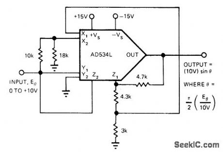
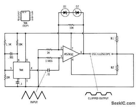
Expression approximating sine function from 0 to 900is generated by function fitting and duplicated by using AD534L analog multiplier and appropriate close.tolerance (0.1%) resistors. Accuracy of sine wave is within ±0.5% at all points. Linearly increasing voltage of triangle develops rising sinusoidal output. Conversely, linearly decreasing input generates mirror of rising sinusoids. Increasing triangle waveform, then bringing it back to zero again, completes full cycle of sine-wave out-put.-R. Frantz, Analog Multipliers-New IC Versions Manipulate Real-World Phenomena with Ease, EDN Magazine, Sept. 5, 1977, p 125-129. (View)
View full Circuit Diagram | Comments | Reading(783)
SUPPRESSED_CARRIER_AM
Published:2009/7/6 22:46:00 Author:May
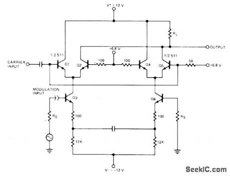
Double-balanced modulator using Signetics 511 transistor array gives output consisting of sum and difference frequencies of carrier and modulation inputs along with related harmonics. Circuit is self-balancing, eliminating need for pots, Output includes small amounts of carrier and modulating signal. Capacitor between emitters of Q3 and Q6 is selected to have low reactance at lowest modulating frequency.- Signetics Analog Data Manual, Signetics, Sunnyvale, CA, 1977, p 750-751. (View)
View full Circuit Diagram | Comments | Reading(912)
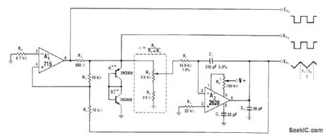
DRIVEN_CONSTANT_AMPLITUDE_SAWTOOTH
Published:2009/7/6 22:44:00 Author:May
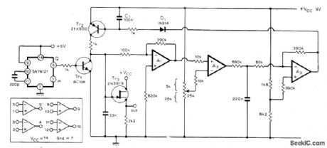
Gives constant-amplitude output over input frequency range of 2-100 kHz. Input signal from SN74121 IC is 300-ns pulse that drives basic sawtooth generator Tr1-Tr2. Resulting sawtooth waveform is amplified by opamp A1 of MC3401P four-opamp package and fed to A2 which acts as comparator for amplitude-sensing, 25K threshold-setting pot is adjusted for maximum linearity of amplitude versus frequency, Rectangular-wave output ofA2 is filtered to give control voltage that is shifted in level by A3 and D1 to meet input voltage requirements of Tr2. Desired sawtooth output appears at source of Tr3.-J. N. Paine, Constant AmplitudeSawtooth Generator, Wireless World, 0ct.1975, p 473. (View)
View full Circuit Diagram | Comments | Reading(765)
Control_of_higher_voltage_motors
Published:2009/7/21 23:48:00 Author:Jessie
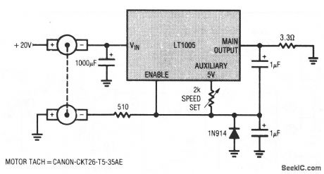
This circuit shows how an LT1005 multifunction regulator can be used to control operation of higher-voltage motors. The circuit is similar to that of Fig. 8-6, except that a 1000-μF capacitor is placed at the regulator to filter transients that are generated by motor switching. When the tach output calls for power, the LTl005 comes on, and allows current to flow through the motor. This forces the LTl005 input toward ground for the duration of the turn-on time. The advantage of this circuit over that of Fig. 8-6 is that higher-voltage motors (up to 20 V) can be used. (View)
View full Circuit Diagram | Comments | Reading(1337)
DELTA_MODULATOR
Published:2009/7/6 22:43:00 Author:May
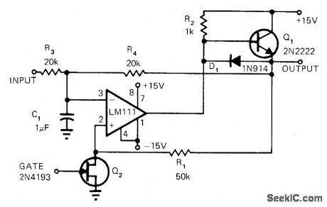
Uses LM111 comparator in basic pulse-ratio modulator circuit, with output pulse width and transition time fixed by external clock signal applied to gate of JFET switch a,. Average value of output is always proportional to input voltage,-R. C. Dobkin, Comparators Can Do More than Just Compare, EDN Magazine , Nov. 1, 1972, p 34-37. (View)
View full Circuit Diagram | Comments | Reading(1481)
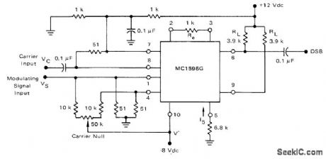
OUBLE_SIDEBAND_SUPPRESSED_CARRIER
Published:2009/7/6 22:41:00 Author:May
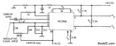
Motorola MC1596G double-balanced modulator has carrier input between pins 8 and 7 and modulation between pins 1 and 4. Balancing carrier-null circuit, also connected between pins 1 and 4, contributes to excellent carrier rejection at output. For unbalanced output, ground one of push-pull output terminals. Requires two supplies.-E. M. Noll, Linear IC Principles, Experiments, and Projects, Howard W. Sams, Indianapolis, IN, 1974, p 138-139. (View)
View full Circuit Diagram | Comments | Reading(796)
Time_delayed_relay_for_up_to_1_minute
Published:2009/7/21 23:47:00 Author:Jessie
Time-delayed relay for up to 1 minute (courtesy General Electric Company). (View)
View full Circuit Diagram | Comments | Reading(722)
20_20000_Hz_SQUARE_TRIANGLE
Published:2009/7/6 22:38:00 Author:May
Rt and Ct are chosen for upper frequency limit of 20 kHz,and oscillator is adjustable down to lower limit of 20 Hz with R5Circuit will operate up to 100 kHz if component values are suitably changed.A2should be offset-nulled by adjusting for best symmetry at lowest frequency. Total width of T of output waveform varies between 50 μs and 50 ms at frequency range covered.-W. G. Jung, IC Op-Amp Cookbook, Howard W. Sams, Indianapolis, IN, 1974, p 381-383. (View)
View full Circuit Diagram | Comments | Reading(744)
Line_operated_level_switch
Published:2009/7/21 23:46:00 Author:Jessie
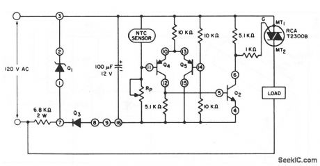
This circuit uses a CA3096 or CA3096A transistor array to control a triac. (View)
View full Circuit Diagram | Comments | Reading(1015)
8_digit_up_down_counter_using_two_cascaded_ICM7217_28_pin_DIPs
Published:2009/7/21 23:46:00 Author:Jessie
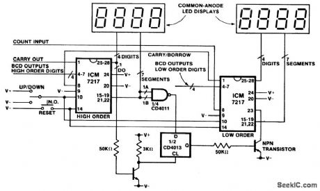
8-digit up/down counter using two cascaded ICM7217 28-pin DIPs. The NAND gate whether a digit is active since one of the two segments not-a or not-b is active on any unblanked number. The flip-flop is clocked by the LSB of the higher-order counter so if this digit is unblanked the Q output of the flip-flop goes high and turns on the NPN transistor, inhibiting leading zero blanking on the lower-order counter (courtesy Intersil, Inc.). (View)
View full Circuit Diagram | Comments | Reading(2979)
On_off_touch_switch
Published:2009/7/21 23:44:00 Author:Jessie
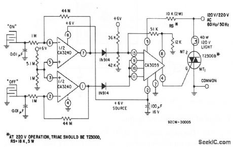
This circuit uses a CA3240E to sense small currents flowing between contact points on a touch plate, which consists of a PC board metalization grid. When the On plate is touched, current flows between the two halves of the grid, and causes a positive shift in the output voltage (pin 7) of the CA3240E. These positive transitions are fed into the CA3079, which is used as a latching circuit and zero-crossing triac driver. When pin7 of the CA3240 is positive, the triac and lamp are on. The opposite occurs when the Off plate is touched, and pin 1 of the CA3240 is positive. (View)
View full Circuit Diagram | Comments | Reading(2542)
Temperature_controller
Published:2009/7/21 23:41:00 Author:Jessie
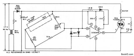
This circuit shows a CA3094B and triac that are connected to form a temperature controller. (View)
View full Circuit Diagram | Comments | Reading(1841)
Presettable_analog_timer
Published:2009/7/21 23:39:00 Author:Jessie
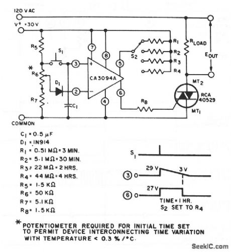
This circuit shows a CA3094A and triac connected to form a presettabletimer. The time is preset by the selected values of R1 through R4. (View)
View full Circuit Diagram | Comments | Reading(730)
100_MHz_multifunction_counter_using_an_Intersil_ICM7216A_28_pin_DIP
Published:2009/7/21 23:37:00 Author:Jessie

100 MHz multifunction counter using an Intersil ICM7216A 28-pin DIP (courtesy lntersil, Inc.). (View)
View full Circuit Diagram | Comments | Reading(996)
PPM_WITH_ANALOG_CONTROL_OF_DELAY
Published:2009/7/6 22:37:00 Author:May

Opamp, UJT, and two TTL packages generate pulse whose delay, following sync pulse, is con-trolled by amplitude of analog input signal at time of sync pulse. Opamp precharges timing capacitor to level depending on analog signal. Sync pulse disconnects opamp, after which timing capacitor charges up to UJT firing point .UJT output pulse then resets circuit, giving de-sired delayed output pulse through 9601 mono MVBR,-J. Taylor, Analog Signal Controls Pulse Delay, EDN Magazine, Feb. 5, 1974, p 96. (View)
View full Circuit Diagram | Comments | Reading(1387)
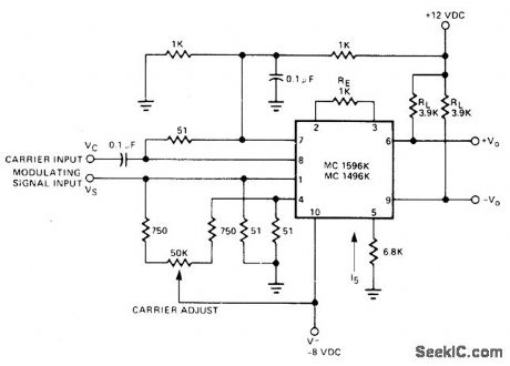
DSB_BALANCED_MODULATOR
Published:2009/7/6 22:33:00 Author:May
Provides excellent gain and carrier suppression by operating upper (carrier) differential amplifiers of Motorola MC1596G balanced modulator at saturated level and lower differential amplifier in linear mode. Recommended input levels are 60 m VRMS for carrier and 300 m VRMS maximum for modulating signal.-R. Hejhall, Input MC1596 Balanced Modulator, Motorola, Phoenix, AZ, 1975, AN-531, p 3. (View)
View full Circuit Diagram | Comments | Reading(775)
SINGLE_IC_AM
Published:2009/7/6 22:30:00 Author:May
Adjustable carrier offset is added to carrier differential pairs to provide car-rier-frequency output that varies in amplitude with strength of modulation signal - Signetics Analog Data Manual, Signetics, Sunnyvale, CA, 1977, p 757. (View)
View full Circuit Diagram | Comments | Reading(721)
| Pages:1012/2234 At 2010011002100310041005100610071008100910101011101210131014101510161017101810191020Under 20 |
Circuit Categories
power supply circuit
Amplifier Circuit
Basic Circuit
LED and Light Circuit
Sensor Circuit
Signal Processing
Electrical Equipment Circuit
Control Circuit
Remote Control Circuit
A/D-D/A Converter Circuit
Audio Circuit
Measuring and Test Circuit
Communication Circuit
Computer-Related Circuit
555 Circuit
Automotive Circuit
Repairing Circuit