
Circuit Diagram
Index 1004
PULSE_TYPE_TRANSISTOR_TESTER
Published:2009/7/21 22:24:00 Author:Jessie

Constant-current drive for pulse-testing of power transistors at maximum power without over heating has three current ranges. A-c signal in phase with collector supply is advanced 88° by phase-shift bridge, to center one-shot mvbr pulse on peak of cc collector supply.-D. H. Breslow, Measuring Parameters by Power Transistor Pulse Techniques, Electronics, 34:1, p 120-122. (View)
View full Circuit Diagram | Comments | Reading(1087)
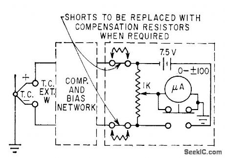
THERMOCOUPLE_AMPLIFIER_WITH_COLD_JUNCTION_COMPENSATION
Published:2009/7/7 2:43:00 Author:May
Input protection circuitry allows thermocouple to short to 120 Vac without damaging the amplifier.
Calibration: 1. Apply a 50 mV signal in place of the thermocouple. Trim R3 for VOUTut 12.25 V. 2. Reconnect the thermocouple. Trim R9 for correct output. (View)
View full Circuit Diagram | Comments | Reading(0)
NONHEATING_THERMOCOUPLE_TESTER
Published:2009/7/21 22:23:00 Author:Jessie
Potentiometer completes bridge circuit of simple lest set that checks thermocouple installations for thermal contact, electrical continuity, and correct polarity, without causing temperature change at thermocouple junction. Operation depends on resistance difference between thermocouple wires, which ranges from 6.5 ohms per 100 feet of 28-gage copper wire to 266 ohms for Chromel-P.-S. Meieran, Tester Chicks Out Thermocouple Circuits, Electronics, 36:11, p 102-106. (View)
View full Circuit Diagram | Comments | Reading(636)
90°_PHASE_SHIFT_WITH_BRIDGES
Published:2009/7/21 22:22:00 Author:Jessie
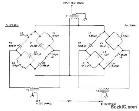
Wideband passive AF phase-shift network makes direct-conversion SSB generation possible. Developed for use with circularly polarized antenna system. Bridge networks each provide 45°phase shift between 1 and 15 MHz, to give differential phase shift of 90° over that frequency range with phase error less than 1°. Amplitude difference between outputs is less than 0.5dB over range. T1, T2, and T3 are wound on Neosid 1050-1-F14 of Indiana General F684-1 balun core. Twist together three 7-inch lengths of No.26 enamel and wind 3 turns through the two holes. Connect two wires in series lot windings going to bridges. Article gives data for winding all other coils.-R. Harrison, A Review of SSB Phasing Techniques, Ham Radio, Jan. 1978, p 52-62. (View)
View full Circuit Diagram | Comments | Reading(1992)
80_W_LINEAR_FOR_MOBILE_SSB
Published:2009/7/7 2:43:00 Author:May

Designed for operation from 12.5-V supply, using driver stage to provide total power gain of about 30 dB for 3-30 MHz band. Negative collector-to-base feedback provides gain compensation in both driver and output stages. Low circuit impedances make layout and construction more critical than with higher-voltage circuits.-H.Granberg, Broadband Linear Power Amplifiers Using Push-Pull Transistors, Motorola, Phoenix, AZ, 1974, AN-593, p 7. (View)
View full Circuit Diagram | Comments | Reading(768)
10_W_ON_2_METERS
Published:2009/7/7 2:41:00 Author:May
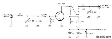
Single TRW PT5757 transistor provides 10-W output when operating from 12.5-V auto battery. L1 is 4 tums No. 20 enamel and L2 is 10 tums No. 20, both with 3/32inch inner diameter. T1 is 4:1 transmission-line transformer made from 3-inch length of twisted-pair No. 20 enameL-J. Fisk, Two-Meter Power Amplifier, Ham Radio, Jan. 1974, p 67. (View)
View full Circuit Diagram | Comments | Reading(802)
CURVATURE_CORRECTED_PLATINUM_RTD_THERMOMETER
Published:2009/7/7 2:41:00 Author:May

This thermometer is capable of 0.01℃ accuracy over -50℃ to + 150℃. A unique trimarrangement eliminates cumbersome trim interactions so that zero gain, and nonlinearity correction can be trimmed in one even trip. Extra op amps provide full Kelvin sensing on the sensor without adding drift and offset terms found in other designs. A1 is configured as a Howland current pump, biasing the sensor with a fixed current. Resistors R2, R3, R4 and R5 form a bridge driven into balance by A1. In balance, both inputs of A2 are at the same voltage. Since R6 = R7, A1 draws equal currents from both legs of the bridge. Any loading of the R4/R5 leg by the sensor would unbalance the bridge ; therefore, both bridge taps are given to the sensor open circuit voltage and no current is drawn. (View)
View full Circuit Diagram | Comments | Reading(884)
D_C_LEVEL_SHIFTER
Published:2009/7/21 22:22:00 Author:Jessie

Provides adjustable shift of up to 18 v in d-c voltage level of signal. -T. Mollinga, D-C Level Shifter Checks New Computer Modules, Electronics, 35:27, p 44-45.
(View)
View full Circuit Diagram | Comments | Reading(1)
RS_232_TO_CMOS_LINE_RECEIVER
Published:2009/7/7 2:40:00 Author:May
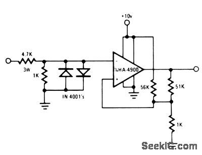
This RS-232 type line receiver to drive CMOS logic uses a Schmitt-trigger feedback network to give about 1-V input hysteresis for added noise immunity. A possible problem in an interface which connects two pieces of equipment, each plugged into a different ac receptacle, is that the power line voltage might appear at the receiver input when the interface connection is made or broken. The two diodes and a 3-W input resistor will protect the inputs under these conditions.
(View)
View full Circuit Diagram | Comments | Reading(1087)
2_METER_QRP
Published:2009/7/7 2:39:00 Author:May

Can supply up to 1W of RF out-put on CW for portable or low-power (QRP) amateur radio operation. Provides chirpless keying with negligible backwave. Operates from 12-V car battery or lantern batteries. Oscillator uses 7-MHz fundamental crystal and 40080 transistor al, with 40081 in final stage. L1 is 20 turns No.28 on 1/4-inch slug-tuned form. L3 is 28 turns No.28 on 1/4-inch slug-tuned form, with 5 turns No.24 wound on it for L2 and the same for L4. Article covers construction and operation.-C. Klinert, Simple QRP Transmitter, 73 Magazine, Aug. 1973, p 65-67. (View)
View full Circuit Diagram | Comments | Reading(1580)
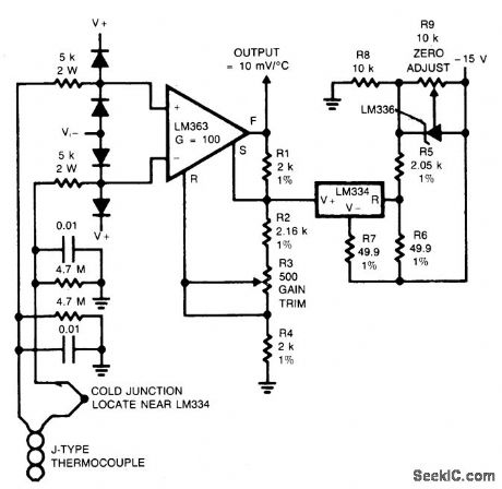
TEMPERATURE_SENSOR_AND_DVM_INTERFACE
Published:2009/7/7 2:39:00 Author:May

The DVM gives a direct indication of the temperature of the sensor in degrees Centigrade. The temperature sensor IC1 gives a nominal 1 μA per degree Kelvin which is converted to 10 mV per degree Kelvin by R1 and VR1. IC2 is a micropower, low input drift op amp with internal voltage reference and amplifier. The main op amp in IC1 is connected as a voltage follower to buffer the sensor voltage at R1.The second amplifier in IC1 is used to amplify the.2 V internal reference up to 2.73 V in order to offset the 273 degrees below 0℃. The output voltage of the unit is the differential output of the two op amps and is thus equal to 0.01 V per ℃. (View)
View full Circuit Diagram | Comments | Reading(956)
SINE_SQUARE_TRIANGLE_AT_3_5_V
Published:2009/7/7 2:38:00 Author:May

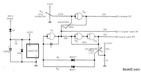
Uses CD4011 IC operating from 1 5-V AC Iine as at left.NAND gates of IC are connected as at right, with G1serving as integrator with variable delay time, G2-G3as Schmitt trigger, and G4as triangle to sine-wave converter.Sine-wave approximation, depending on transf er function of G4,is calibrated by R3and R4.Values of R1and R2 may be varied between 0.01 and 10 megohms and C between 100 pF and 2.2 μF to obtain desired sawtooth and pulse waveforms at desired frequency determined by setting of R5.-J. W.Richter, Single L.C. Function Generator, Wireless World, Nov. 1976, p 61. (View)
View full Circuit Diagram | Comments | Reading(992)
Zero_crossing_switch_with_SCR_slave_configuration
Published:2009/7/21 22:22:00 Author:Jessie
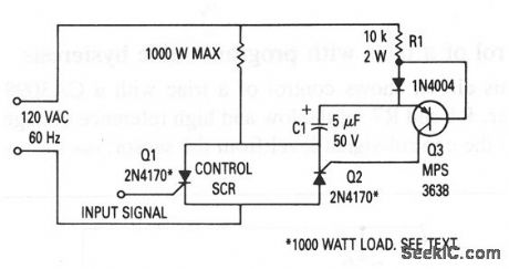
This circuit provides a single pulse to the gate of SCR Q2 each time that SCR Q1 turns on, thus turning Q2 on for the half-cycle following the half-cycle during which Q1was on. Q2 is turned on only when Q1 is turned on, and the load can be controlled by a signal applied to the gate of Q1. The control signal can be either dc or a power pulse. The SCR used must be capable of handling the maximum current requirements of the load to be driven. The 8-A 200-V SCRs shown will handle a 1-kW load. 2N6397s can also be used in this circuit, and will hands up to 12 A. (View)
View full Circuit Diagram | Comments | Reading(897)
MULTIPLEINPUT_DETECTOR
Published:2009/7/7 2:38:00 Author:May
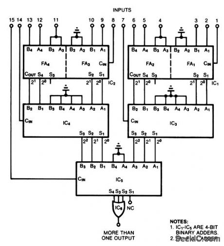
This circuit determines whether more than one input in a group of digital inputs is active. It provides a digital measure of the number of active inputs, and it allows you to establish a threshold for majority-decision applications. That is, whether the number of active inputs is more than, less than, or equal to a value between 1 and 15. You can monitor more inputs by cascading the adders.
Each binary adder, IC1 and IC2, forms two full adders (FAs). Each FA monitors three input lines and generates a 2-bit output representing the number of inputs active. IC3 and IC4, by summing the outputs of two FAs plus an input line, individually measure how many in a group of seven inputs are active. Similarly, by monitoring the 3-bit outputs of IC3 and IC4 plus one input, IC5 measures how many in the group of 15 are active. The OR gate, IC6, simply indicates whether more than one input is active. (View)
View full Circuit Diagram | Comments | Reading(819)
INDUCTIVE_TELEMETRY_FOR_ROTATING_TEST_FIXTURE
Published:2009/7/21 22:21:00 Author:Jessie

Transducer, oscillator, modulator, and battery supply rotate with device under test. Carrier frequency of 1 Mc, modulated over range of 200 to 10,000 cps, is transferred inductively from rotating output coils L1-L2 to stationary pickup coils.-H. Baumann, Inductive Telemetry Improves Spin-System Measurements, Electronics, 36:46, p 41-42. (View)
View full Circuit Diagram | Comments | Reading(742)
DUAL_OUTPUT,OVER_UNDER_TEMPERATURE_MONITOR
Published:2009/7/7 2:37:00 Author:May
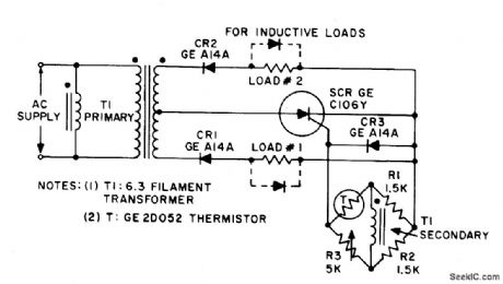
This circuit is ideal for use as an over-under temperature monitor, where its dual output feature can be used to drive HIGH and LOW temperature indicator lamps, relays, etc. T1 is a 6.3 volt filament transformer whose secondary winding is connected inside a four arm bridge. When the bridge is balanced, ac output is zero, and C5 (or C7) receives no gate signal. If the bridge is unbalanced by raising or lowering the thermistor's ambient temperature, and ac voltage will appear across the SCR's gate cathode terminals. Depending in which sense the bridge is unbalanced, the positive gate voltage will be in phase with, or 180° out of phase with the ac supply. If the positive gate voltage is in phase, the SCR will deliver load current through diode CR1 to load (1), diode CR2 blocking current to load (2). Conversely, if positive gate voltage is 180° out of phase, diode CR2 will conduct and deliver power to load (2), CR1 being reverse biased under these conditions. With the component values shown, the circuit will respond to changes in temperature of approximately 1-2℃. Substitution of other variable-resistance sensors, such as cadmium sulfide light dependent resistors (LDR) or strain gauge elements, for the thermistor shown is permissible. (View)
View full Circuit Diagram | Comments | Reading(678)
CARRIER_OSCILLATOR
Published:2009/7/21 22:20:00 Author:Jessie

Two MOSFETs serve with diode switching arrangement for selecting either upper or lower sideband. Circuit between gates couples oscillator to isolating output stage. Upper/lower sideband switch applies +9V to anode of switching diode that closes feed-back circuit for crystal to be activated. Output can be used as injection voltage in demodulation of incoming signal by product detector of transceiver or as basic carrier applied to balanced modulator for transmitting mode. Used in SSB transceiver made by Sideband Associates for radio marine communication in 2-23 MHz range.-E. Noll, MOSFET Circuits, Ham Radio, Feb. 1975, p 50-57. (View)
View full Circuit Diagram | Comments | Reading(943)
MICROPROCESSOR_CONTROLLEDANALOG_SIGNAL_ATTENUATOR
Published:2009/7/7 2:36:00 Author:May

View full Circuit Diagram | Comments | Reading(939)
ADJUSTABLE_THRESHOLD_TEMPERATURE_ALARN
Published:2009/7/7 2:35:00 Author:May

When R1 increases as temp decreases, the output of IC1 goes positive, turning on Q1. Q1 conducts and causes Q2 to conduct, turning on the audible alarm. The threshold is set with potentiometer R2. (View)
View full Circuit Diagram | Comments | Reading(1155)
CURRENT_PULSE_GENERATOR
Published:2009/7/21 22:19:00 Author:Jessie
Used for production testing of ferrite memory cores. Provides pulse amplitudes from 200 ma to 3 amp at repetition rates up to 20 kc.-H. W. Goss, Current Pulse Generator Tests Magnetic Cores, Electronics, 33:1, p 80-81. (View)
View full Circuit Diagram | Comments | Reading(1195)
| Pages:1004/2234 At 2010011002100310041005100610071008100910101011101210131014101510161017101810191020Under 20 |
Circuit Categories
power supply circuit
Amplifier Circuit
Basic Circuit
LED and Light Circuit
Sensor Circuit
Signal Processing
Electrical Equipment Circuit
Control Circuit
Remote Control Circuit
A/D-D/A Converter Circuit
Audio Circuit
Measuring and Test Circuit
Communication Circuit
Computer-Related Circuit
555 Circuit
Automotive Circuit
Repairing Circuit