
Circuit Diagram
Index 1005
1_4_W_CW_TRANSMITTER
Published:2009/7/7 2:35:00 Author:May

Low-power two-stage FET transmitter for 80-meter amateur band uses Pierce crystal oscillator that requires no output resonant ci.rcuit. DC milliammeter can be connected across 150-ohm resistor in gate circuit of second transistor to indicate strength of oscillator output signal, Resonant circuit of RF amplifier Q2 uses toroid L2 (56turns No, 24 enamel 13/16-in Permacor 57-1541 core) and two series-connected trimmers. Milliam-meter is connected across C8 when level of BF output voltage js to be measured.-E. M. Noll, FET Principles, Experiments, and Projects, Howard W. Sams, Indianapolis, IN, 2nd Ed., 1975,p 204-207. (View)
View full Circuit Diagram | Comments | Reading(2594)
TWO_TONE_BURSTS
Published:2009/7/21 22:19:00 Author:Jessie
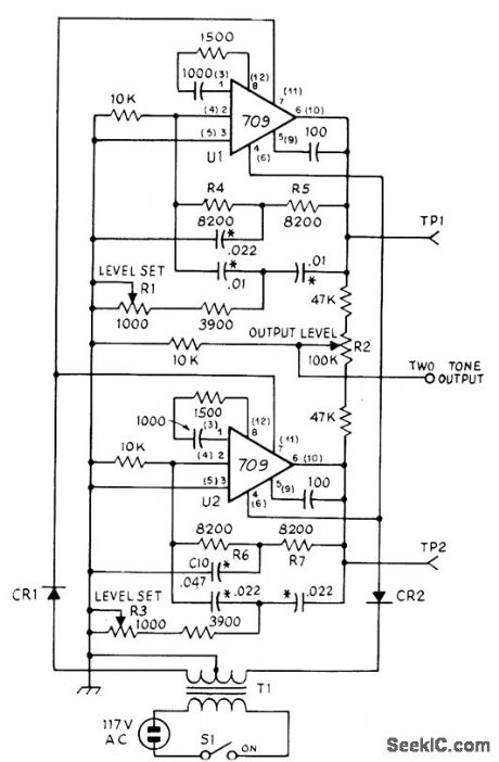
Uses 709 or 741 opamps to generate 1850-Hz and 855-Hz tones simulta-neously, pulsed at 60-Hz line rate for duty cycle slightly below 50%. Used to measure linearity of high-frequency amplifiers in low-power stages of SSB transmitter. Each opamp is pow-ered by half-wave rectified AC, with opposite voltage polarities provided by 12.6-V CT 50-mA filament transformer, Tone frequency of each opamp is determined by symmetrical twin-T network. R1 sets level of 1850-Hz tone, and R3 controls 855-Hz tone. R2 mixes and balances tones. Diodes are 50-PIV 500-mA silicon.-B. Buus, A Technique for Burst Two-Tone Testing of Linear Amplifiers, QST, Aug. 1971, p17-21. (View)
View full Circuit Diagram | Comments | Reading(683)
Zero_crossing_switch_for_nonsensitive_gate_SCRs
Published:2009/7/21 22:19:00 Author:Jessie
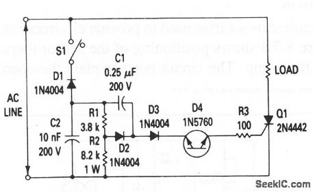
This circuit is primarily for nonsensitive-gate SCRs, such as the 2N4442 (or an MCR218-8), and loads of 8.0 A or less. (View)
View full Circuit Diagram | Comments | Reading(905)
ONE_OF_EIGHT_CHANNEL_TRANSMISSION_SYSTEM
Published:2009/7/7 2:35:00 Author:May
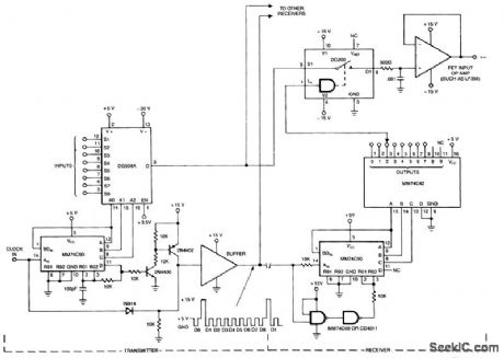
View full Circuit Diagram | Comments | Reading(1020)
TEMPERATURE_ALARM
Published:2009/7/7 2:34:00 Author:May
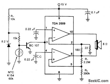
The mute pin of this dual audio amplifter is so used as the trigger for a one chip high-temperature alarm. One-half of the IC is connected as an oscillator and the other boosts the audio alarm outputs to 10W. (View)
View full Circuit Diagram | Comments | Reading(978)
DUAL_TIMER_CHIP_CONTROLS_TEMPERATURE_WHILE_MONITORING_LIQUID_LEVEL
Published:2009/7/7 2:32:00 Author:May
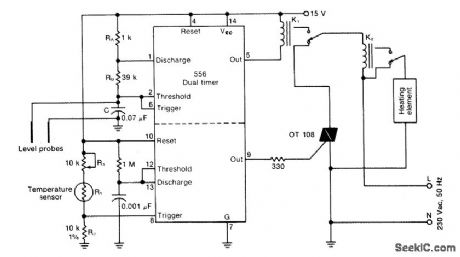
One-half of a 556 dual timer monitors the temperature of a liquid bath, controlling a heating element that maintains temperature within ±2℃ over a 32℃- 200℃ range.The other half monitors the liquid level, disconnecting the heater when the level drops below a preset point. (View)
View full Circuit Diagram | Comments | Reading(1075)
FACSIMILE_PHASE_CONTROL
Published:2009/7/7 2:31:00 Author:May

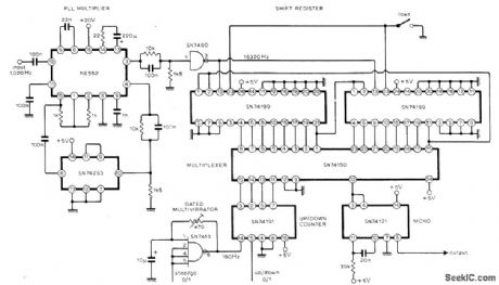

Circuit provides accurate phasing of 51-polpair phonic/synchronous motor in facsimile transmitter, and can readily be adapted for similar applications. A 16-stage shift register loaded with 1 bit and connected as ring counter is clocked at 16 times required drive motor frequency. This gives pulse train with 1:15 mark-space ratio and repetition rate equal to drive frequency. Multiplexer used as single-pole 16-way switch can select output for any stage of shift register; each clockwise switch step gives 360/16 or 22.5° phase advance. Article describes circuit operation in detail-P. E. Baylis and R. J. Brush, Synchronous-Motor Phase Control, Wireless World, April 1976, p 62. (View)
View full Circuit Diagram | Comments | Reading(1530)
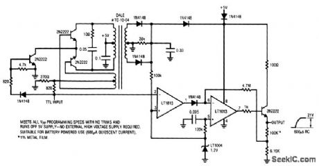
5V_POWERED_EEPROM_PULSE_GENERATOR
Published:2009/7/7 2:25:00 Author:May
View full Circuit Diagram | Comments | Reading(579)
RGB_BLUE_BOX
Published:2009/7/7 2:23:00 Author:May
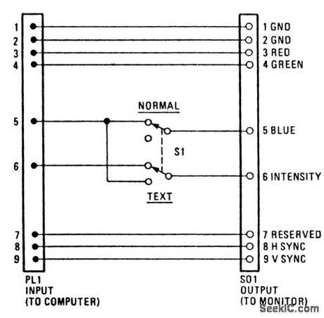
The RGB blue box turns your PC's RGB-moni-tor screen blue at the flip of a switch. That is, it makes your computer display bright white text on a blue background, instead of the usual low-intensity white on black. The RGB blue box connects between your IBM PC color graphics adapter, or equivalent, and your RGB color monitor. By flipping a switch, you choose between two modes. One mode passes the signal from the PC to the monitor unaltered; the other transforms it to make text more readable. The monitor has four TTL-level inputs-red, green, blue, and intensity-and it interprets disconnected wires as on. That's why the screen turns white if you disconnect the monitor from the computer, and blue if you disconnect only the blue line. Instead of just discarding the blue signal,the blue box reroutes it to the intensity input. As a result, most of the text colors come out intensified.
(View)
View full Circuit Diagram | Comments | Reading(731)
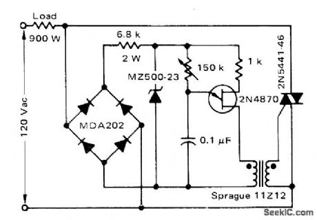
900_W_FULL_WAVE_TRIGGER
Published:2009/7/7 2:22:00 Author:May

Uses UJT for phase control of triac. Suitable for control of shaded-pole motors driving loads having low starting torque, such as fans and blowers.-D.A. Zinder, Electronic Speed Control for Appliance Motors, Motorola, Phoenix, AZ, 1975, AN-482,p4. (View)
View full Circuit Diagram | Comments | Reading(1417)
PHASING_TYPE_SSB_GENERATOR
Published:2009/7/21 23:14:00 Author:Jessie
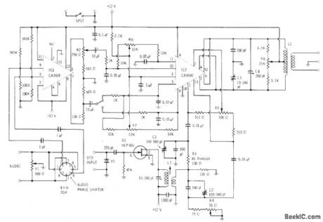
Modulating wave is first applied to input audio phase shifter for generating audio components that are equal in magnitude but differ 90°in phase. After amplification in CA3018, these audio components are applied to CA3050 double-balanced modulator. SPST and SPDT switch settings determine which sideband will appear at output of modulator. Carrier is generated by FET crystal oscillator for application through RF phase-shift network to pins 1 and 13 of modulator. Both carrier and modulating frequencies are suppressed in balanced output circuit of modulator, leaving only desired sideband. Resonant output transformer provides low-impedance feed to succeeding linear amplifier. Designed for 160-meter band.-E. M. Noll, Linear IC Principles, Experiments, and Projects, Howard W. Sams, Indianapolis, IN, 1974, p 356-357. (View)
View full Circuit Diagram | Comments | Reading(1574)
INTERFACE_TO_680X_650X_AND_8080_FAMILIES
Published:2009/7/7 2:21:00 Author:May
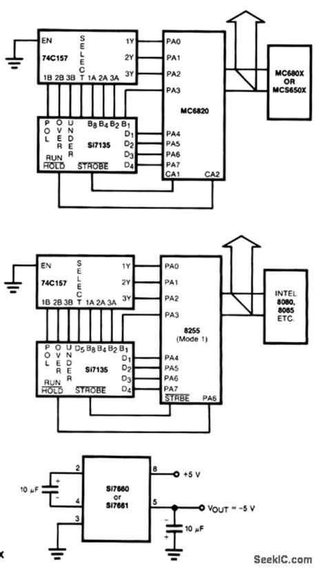
Circuits to interface the Si7135 directly with two popular microprocessors are shown in Figs. 18-2a and b. The 8080/8048 and the MC6800 families with 8-bit words need to have polarity, overrange, and underrange multiplexed onto the digit 5 word. In each case, the microprocessor can instruct the ADC when to begin a measurement and when to hold this measurement. The Si7135 is designed to work from ±5 V supplies. However, if a negative supply is not available, it can be generated using 2 capacitors, and an inexpensive Si7660 or Si7661 IC, as shown in Fig. 18-2c. (View)
View full Circuit Diagram | Comments | Reading(575)
Programmable_100_hour_timer_with_display
Published:2009/7/21 23:00:00 Author:Jessie
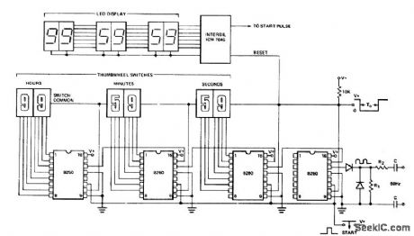
Programmable 100-hour timer with display. The 8260 on the right uses the carryout gate to generate a t -second clock from the 60-hertz line. The diodes on the time base input rectify the input signal and alternately clamp and release the internal pull-up resistor at pin 14. The input network depends on the amplitude of the 60-hertz signal available. The internal oscillators are disabled with a t K resistor at pin 13. The second and third 8260s are programmable with thumbwheel switches up to 59 seconds and 59 minutes. The carryout of each divider drives the next counter. The 8250 was chosen to give the maximum count of 99 hours. All request pins are tied together and back to the 10K output pull-up resistors at the thumbwheels. The timing cycle begins by pressing the pushbutton. The 7045 provides a counter chip pulse direct drive to the 7-segment LEDs. Timing resolution can be increased to hundredths of a second by substituting 8250s for the initial stages and using the 60-hertz line to generate a 100-hertz clock (courtesy Intersil, Inc.). (View)
View full Circuit Diagram | Comments | Reading(1868)
LOW_LEVEL_CMOS_COIVTROL
Published:2009/7/7 2:16:00 Author:May
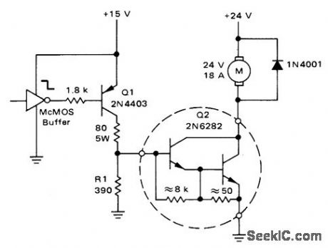
Low-level output of CMOS buffer turns on DC motor through Q1 and 20-A Darlington power transistor Q2.-A. Pshaenich,” Interface Techniques Between Industrial Logic and Power Devices,” Motorola, Phoenix, AZ, 1975, AN-712A, p 18. (View)
View full Circuit Diagram | Comments | Reading(938)
AUTOMATIC_RS_232_DATASELECTOR
Published:2009/7/7 2:15:00 Author:May
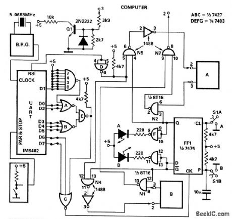
With this dataselector, only one RS-232 port is used to connect two RS-232 devices (i.e., printer, plotter, etc.) with a mini- or microcomputer. The operation is very simple. Power on will reset FFI (QFFI = Low), which enables gates N1, NS, and N7. Now communication between computer and device B is possible. Detection of the switch command, i.e., Control B character = CHR$(2), selectable with wirewrap pins, on the parallel outputs of the UART (IM 6402 or equivalent) will set: QFFI= High. Gates N2, N5, and N7 are open, so device A is connected with the computer until Control B character is detected again.
Transistor Q1 converts RS-232 levels to TTL levels while two LEDs indicate whether device A or B is linked. The baud-rate generator provides the 16 x clock needed for the UART. Any baud rate ranging from 50 to 19200 can be selected. Manual control of the selector is available with toggleswitch S1.
(View)
View full Circuit Diagram | Comments | Reading(904)
Improved_lamp_dimmer
Published:2009/7/21 22:59:00 Author:Jessie
This circuit is an improved version of the circuit shown in Fig. 8-21. The hysteresis effect is eliminated by the addition of two diodes and the 5.1 -kΩ resistor. The RC network across the triac is a snubber to prevent line transients from accidentally firing the triac. The circuit operates from a 120-V 60-Hz source, and can control up to 1000 W of power to incandescent bulbs (but not fluorescents). (View)
View full Circuit Diagram | Comments | Reading(2152)
SHUNT_WOUND_MOTOR
Published:2009/7/7 2:12:00 Author:May
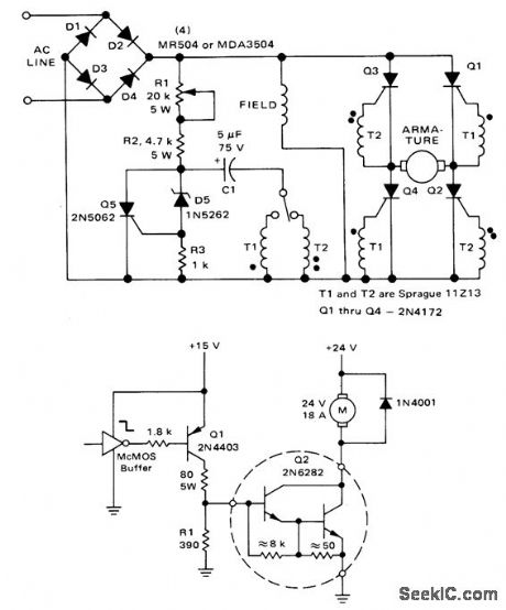
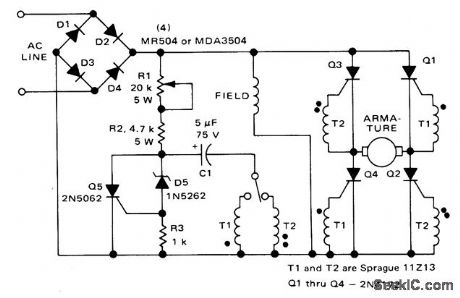
Switch provides direction control and R1 controls speed of fractional-horsepower shunt-wound DC motor. Field is placed across rectified supply, and armature windings are in four-SCR bridge circuit. Switch determines which diagonal pair of SCRs is turned on, to control direction of rotation. Triggering circuit consisting of Q5, D5, and C1 is controlled by R1, for changing conduction angle of triggered SCR path.- Direction and Speed Control for Series, Universal and Shunt Motors, Motorola, Phoenix, AZ, 1976, AN443. (View)
View full Circuit Diagram | Comments | Reading(4315)
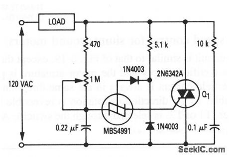
Low_cost_lamp_dimmer
Published:2009/7/21 22:56:00 Author:Jessie
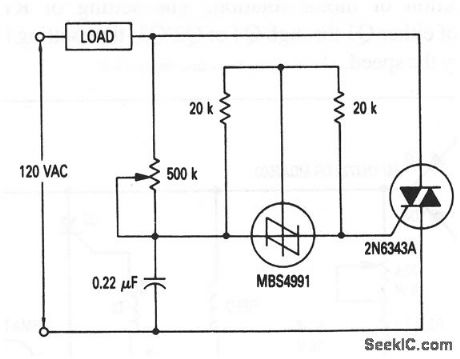
This circuit shows a full-range, low-cost, lamp dimmer that uses an MBS4991 silicon bilateral switch (SBS) to trigger the triac. The two 20-kΩ shunt resistors minimize the flash-on or hysteresis effect of the SBS, and improve the temperature sensitivity. (View)
View full Circuit Diagram | Comments | Reading(0)
14_W_BROADBAND_LINEAR_FOR_7_AND_14MHz
Published:2009/7/7 2:10:00 Author:May
Requires about 10-mW driving power. Frequency responseis essentially flat over 7-14 MHzfrequency range Diodes are 1N4003,Q8 is 2N2222A、Q9 is 2N3866, Q10 is 2N2270,and Q11 is 2N4037. RF chokes use 18turns No. 28 enamel on FT-37-43 ferrite toroid core. Primary of T2 is 30 turns of No. 28 enamel on FT-50-43 ferrite toroid core, with 4 turns No. 28 wound over cold end for secondary. T3 has 16 tums of No. 28 enamel for primary and 4 tums for secondary looped through BLN-43-302 ferrite core. Article gives test procedure.-D. DeMaw, Transmitter Design-Emphasis on Anatomy, QST, July 1978, p 23-25. (View)
View full Circuit Diagram | Comments | Reading(2511)
LEAKAGE_TESTER
Published:2009/7/21 22:31:00 Author:Jessie
Operational trigger trips when transistor leakage is above 5 ma. Response time is 40 millisec.-P. Lefferts, Operational Trigger For Precise Control, Electronics, 37:28, p 50-55. (View)
View full Circuit Diagram | Comments | Reading(939)
| Pages:1005/2234 At 2010011002100310041005100610071008100910101011101210131014101510161017101810191020Under 20 |
Circuit Categories
power supply circuit
Amplifier Circuit
Basic Circuit
LED and Light Circuit
Sensor Circuit
Signal Processing
Electrical Equipment Circuit
Control Circuit
Remote Control Circuit
A/D-D/A Converter Circuit
Audio Circuit
Measuring and Test Circuit
Communication Circuit
Computer-Related Circuit
555 Circuit
Automotive Circuit
Repairing Circuit