
Circuit Diagram
Index 1011
Universal_motor_control_with_built_in_self_timer
Published:2009/7/21 23:28:00 Author:Jessie
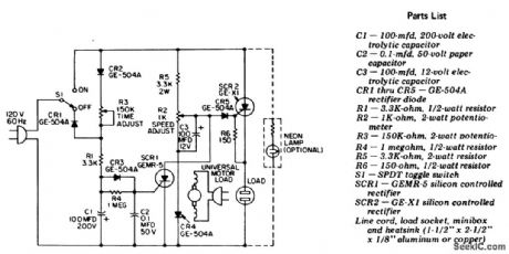
Universal motor control with built-in self-timer. Use this circuit only with motors having commutators. If heavy motor loads are anticipated, use a larger-rated C30B SCR in place of the GE-X1 for SCR2. To increase the time delay increase the capacitance of 01 (courtesy General Electric Company). (View)
View full Circuit Diagram | Comments | Reading(0)
SQUARE_WAVE_MODULATOR
Published:2009/7/6 23:38:00 Author:May
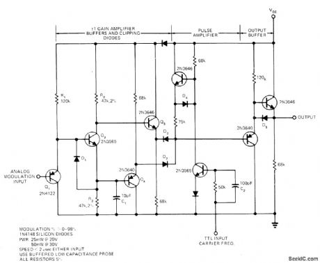
Analog modulation input goes through buffer Q1,-R1, to amplifier Q2-R2,-R3,. Outputs of Q2 are buffered by separate emitter-followers Q3, and Q4, and fed to clipping diodes D2, and D3 acting on top and bottom of amplified carrier wave, Following pulse amplifier converts TTL signal to square wave. Two opposed emitter-followers and D5, form buffer that can either source or sink current from load. Other three diodes are used to speed up circuit operation,Provides modulation range of 0-98%.-E .Burwen, Low-Power Square-Wave Modulator Is TTL Compatible. EDN Magazine.Nov,20.1973,p 91 and 93 (View)
View full Circuit Diagram | Comments | Reading(838)
1_kHz_SINE_SQUARE
Published:2009/7/6 23:32:00 Author:May
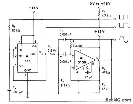
555 timer starts as astable MVBR but then acts withA2 to form multiple-feedback bandpass filter that removes harmonics from square wave to give sine-wave output with distortion less than 2%. Sine output is fed back to timer through C4 which now operates as Schmitt trigger, shaping sine wave to give output square wave. Frequency is determined primarily by filter components C1 C2 R1, and R2. Output is about 9 V P-P.-W. G. Jung, IC Timer Cookbook, Howard W. Sams, Indianapolis, IN, 1977, p 203-204. (View)
View full Circuit Diagram | Comments | Reading(3895)
MOSFET_BALANCED_MODULATOR
Published:2009/7/6 23:30:00 Author:May


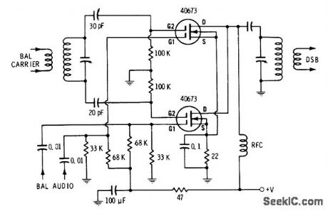
Balanced carrier is fed to G2 gates and balanced audio to G1 gates.Both carrier and audio are canceled in output, leaving desired double-sideband signal.-E.M Noll, ”FET Principles. Experiments, and Projects. ”Howard W .Sams, Indianapoils, IN,2nd Ed,1975,p 195. (View)
View full Circuit Diagram | Comments | Reading(1097)
HYPERBOLIC_SINE
Published:2009/7/6 23:27:00 Author:May
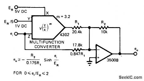
Burr-Brown 4302 multifunction converter and opamp generate hyperbolic sine transfer function with response matching ideal curve within 0.7%. Technique permits setting powers and roots at fractional as well as integer values. Converter shown is set for exponent of 3.2. Choice of amplifier gain and ref erence voltage scales response for given input and output signal levels. Article gives design equations.-J. Graeme, Sinh Generator Boasts 0.7% Error, END Magazine, Aug. 5, 1978, p 70 and 72. (View)
View full Circuit Diagram | Comments | Reading(991)
AMPLITUDE_MODULATOR_1
Published:2009/7/6 23:24:00 Author:May
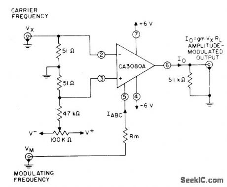
Uses controlled variation of amplifier bias current IABC in CA3080A variable opamp to obtain effective gain control of signal. Variations in amplitude of modulating voltage Vm change bias current through Rm to give amplitude modulation of carrier.- Circuit Ideas for RCA Linear ICs, RCA Solid State Division, Somerville, NJ, 1977, p 15. (View)
View full Circuit Diagram | Comments | Reading(1887)
90_900Hz_SINE_SQUARE_TRIANGGLE_
Published:2009/7/6 23:22:00 Author:May
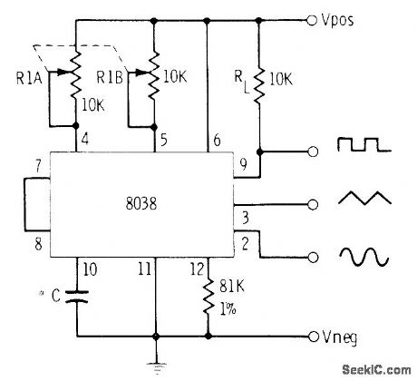
Ganged 10K dual pot covers range when C is 0.25 μF for 8038CC waveform generator. Other values of C (from 0.005,μF to 2.2 μF) give different frequency langes between 10 Hz and 50 kHz. Linearity of waveforms depends on tracking precision of dual pot.-C. D. Rakes, Integrated Circuit Projects, Howard W. Sams, lndianapolis, IN, 1975, p 116-120.
(View)
View full Circuit Diagram | Comments | Reading(827)
PCM_FOR_MICROWAVE_TRANSMITTER
Published:2009/7/6 23:21:00 Author:May
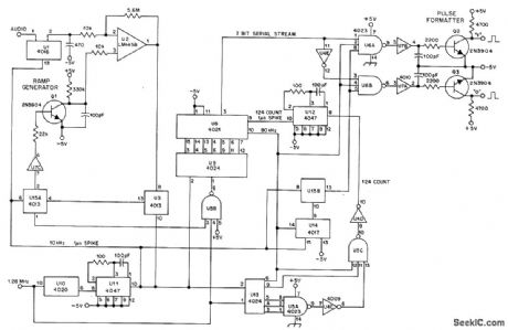
Modern pulse-code modulator can be used for experimentation above lowest legal frequency of 2.3 61ih, such as for satellite and moonbounce communication. Single voice channel is en-coded by using CMOS technology having low power consumption, good noise immunity, and moderate cost. Audio is sampled 10,000 times per second for conversion to 7-pulse code plus synchronizing bit, for 123 levels of encoding frequencies up to 5 kHz, When 10-kHz sampling spike (derived from external 1.28-MHz oscillator by frequency divider U10 and mono U11) arrives at pin 13 of transmission gate U1, AF voltage of pin 1 appears at pin 2.470-pF capacitor charges to this voltage and holds charge until next sample. This voltage is compared by U2 to linear ramp started by Q1 at sampling instant. When ramp voltage exceeds sampled voltage, U2 triggers, setting flip-flop U3 and resetting ramp generator to -5 V. Atsame time, binary counter U9 is stopped by reset flip-flop U15A, and binary equivalent of sample appears at pins 3, 4, 5, 6, 9, 11, and 12 of U9. Remainder of circuit converts bits to serial form for transmission. Article explains circuit operation in detail and gives corresponding decoder circuit for receiver.-V. Biancomano, A Prototype Pulse-Code Modulation System QST, Jan. 1977, p 24.-29. (View)
View full Circuit Diagram | Comments | Reading(4254)
TRANSISTORS_FOR_OSCILLATOR_AND_IF_TUBES
Published:2009/7/6 23:19:00 Author:May

Article covers replacement of tubes in Drake T-4XB transmitter with solid-state equivalent circuits mounted in 7-pin and 9-pin miniature plugs, V4 uses dual-cascode MOSFET,with CR2 and zeners providing highvo ltage protection from keyed grid. Carrier oscillator V5B uses single low-voltage high-p JFET with zener voltage regulator in original grounded plate oscillator circuit. High keyed-ground voltages are isolated by CR3 and B16. Automatic level control amplifier V5A is single high voltage transistor. R14 synthesizes 12AX7 late resistance, to maintain same audio time response.-H. J. Sartori, Solid-Tubes-a New Life for 0ld Designs, 0ST, April 1977, p 45-50. (View)
View full Circuit Diagram | Comments | Reading(1045)
3_kV_AT_2_kW_Deveioped_as_supply_for_1_kW
Published:2009/7/6 23:15:00 Author:May
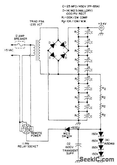
linear ampiifier used in 2-meter moonbounce communication. Article covers construction, with emphasis on insulation requirements, and gives circuit of 1-kW amplifier using Eimac 5-500A pentode.-R. W. Campball, ilowatt Linear Amplifier for 2 Meters, 73 Magazine, Dec. 1973,p29-35. (View)
View full Circuit Diagram | Comments | Reading(631)
1_kHz_SQUARE_TRIANGLE
Published:2009/7/6 23:14:00 Author:May
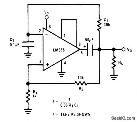
National LM386 opamp operating from 9-V supply generates 1-kHz square wave at 0.5 W for driving 8-ohm loudspeaker or other load. Exact frequency is determined by values used for R1 and C1. Triangle outputcan betaken from pin 2. Pins 1 and 8 can be shorted because DC offset voltages are unimportant.- Audio Handbook, National Semiconductor, Santa Clara, CA, 1977, p 4-30-4-33. (View)
View full Circuit Diagram | Comments | Reading(1221)
100mW
Published:2009/7/6 23:11:00 Author:May
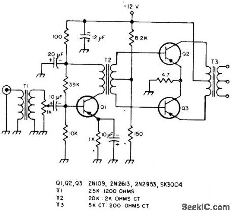
Can be used to collector-modulate transmitters up to about 200 mW or base-modulate somewhat larger power amplifiers. Trans-former coupling minimizes number of components needed.-Circuits, 73 Magazine, Jan.1974, p 177. (View)
View full Circuit Diagram | Comments | Reading(699)
SUPPRESSED_CARRIER_AM_1
Published:2009/7/6 23:09:00 Author:May
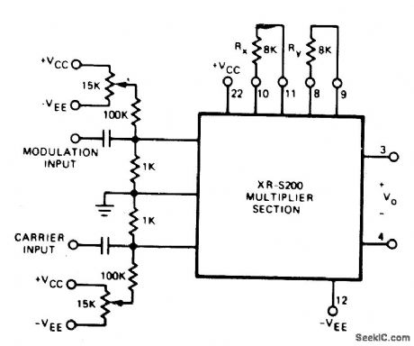
Multiplier section of Exar XR-S200 PLL IC is connected to generate suppressed-carrier AM signal having about 60-dB carrier suppression at 500 kHz and 40 dB at 10 MHz, Inputs are interchangeable.15K offset adjustment pots optimize carrier suppression. Supply voltage range is ±3 to ±30 V.- Phase-Locked Loop Data Book, Exar Integrated Systems, Sunnyvale, CA, 1978, p 9-16. (View)
View full Circuit Diagram | Comments | Reading(821)
DOUBLE_SIDEBAND_SUPPRESSED_CARRIER
Published:2009/7/6 23:06:00 Author:May
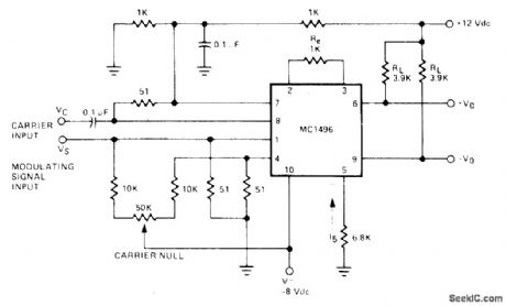
Signetics MC1496 balanced modulator-demodulator transistor array provides carrier suppression while passing sum and difference frequencies. Gain is set by value used for emitter degeneration resistor connected between pins 2 and 3. Output filtering is used to remove unwanted harmonics.- Signetics Analog Data Manual, Signetics, Sunnyvale, CA, 1977, p756-757. (View)
View full Circuit Diagram | Comments | Reading(3398)
VARIABLE_FREQUENCY_AND_RATE
Published:2009/7/21 23:57:00 Author:Jessie
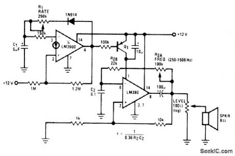
Uses National LM380 opamp as astable oscillator with frequency determined by R2 and C2. Base of Q1 is driven by output of LM3900 opamp connected as second astable oscillator, to turn output of LM380 on and off at rate fixed by R1 and C1. Transistor type is not critical. Circuit is ideal 'tor experimenters.- Audio Handbook, National Semiconductor, Santa Clara, CA, 1977, p 4-21-4-28. (View)
View full Circuit Diagram | Comments | Reading(907)
POLICE_SIREN
Published:2009/7/21 23:56:00 Author:Jessie
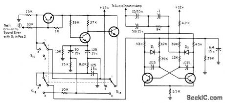
Circuit used in Dietz siren-light police-car system gives distinctive tones. Position t of S1 produces slow continuous rise and fall. Position 3 produces fast rising and falling tone. Position 2 rises slowly to full pitch when point 1 is grounded, then decays at same rate when point 1 is ungrounded. Position 3 gives most noticeable tone for break-in alarm on car. Terminal 1 goes to normally open door, hood, and other switches that complete circuit to ground when opened by intruder. Audio transistors and diode are general replacement types.-J. W. Crawford, The Ultimate Auto Alarm-Model II, CQ, Aug. 1971, p 54-57 and 96. (View)
View full Circuit Diagram | Comments | Reading(252)
Precision_elapsed_time_countdown_timers_using_an_Intersil_ICM7217B_28_pin_DIP
Published:2009/7/21 23:54:00 Author:Jessie
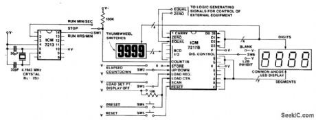
Precision elapsed time/countdown timers using an Intersil ICM7217B 28-pin DIP. This circuit also uses an ICM7213 precision 1-minute/1-second time-base generator to provide a 4.1943 MHz crystal oscillator and divider, generating pulses counted by the ICM7217B, which is a 5959-maximum-count device. The thumbwheel switches allow a starting time to be entered into the counter for a preset countdown type timer, and allow the register to be set for compare functions. For instance, to make a 24-hour clock with BCD output the register can be reset with 2400 and the equals output used to reset the counter (courtesy Intersil, Inc.). (View)
View full Circuit Diagram | Comments | Reading(2298)
Inexpensive_frequency_counter_tachometer
Published:2009/7/21 23:51:00 Author:Jessie
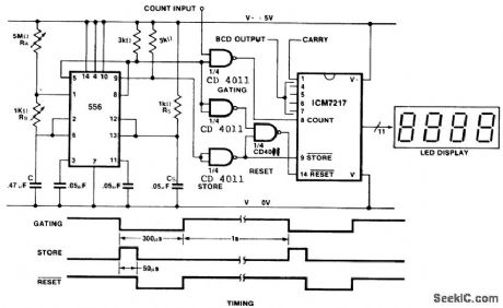
Inexpensive frequency counter/tachometer. This circuit uses a 556 dual timer to generate the gating, not-store and not-reset signals for a ICM7217 counter. One timer is an astable multivibrator using RA, RB and C to provide an output that is positive for approximately 1 second and negative for approximately 300 to 500 μs to serve as the gating signal. The system is calibrated by using a 5M pot for RA as a coarse control and a 1 K pot for RB as a fine control. The other timer is a one-shot multivibrator triggered by the negative-going edge of the gating. This output at pin 9 is inverted to serve as the store pulse and to hold not-reset high. When the one-shot times out and the store goes high, not-reset goes low, resetting the counter. The one-shot pulse width is approximately 50 μs with the components shown. When fine trimming with FIB care should be taken to keep the gating low time at least twice as long as the one-shot pulse width (courtesy Intersil, Inc.). (View)
View full Circuit Diagram | Comments | Reading(1)
30_20000Hz_SQUARE_TRIANGLE_
Published:2009/7/6 23:05:00 Author:May
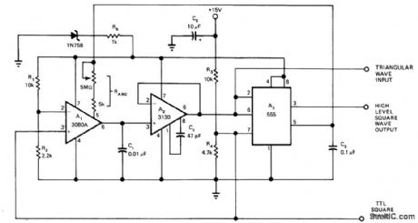
Uses 555 timer as bilevel threshold detector, together with A1 as bidirectional constant-current source an A1 charges Ct between +5 and +10 V threshold points of 555 to give Iinear triangle output for buffering by A2. Simultaneously, toggling of 555 between its high and low output generates square wave of about 13 V at pin 3, along with 5-V TTL output at ρin 7 for additional squarewave output and for contrailing state of A1.-W G,Jung,Build a Function Generator with a 555 Timer,EDN Magazine,Oct.5,1976,p 110. (View)
View full Circuit Diagram | Comments | Reading(951)
100_MODULATION_OF_DIGITAL_SIGNALS
Published:2009/7/6 23:02:00 Author:May
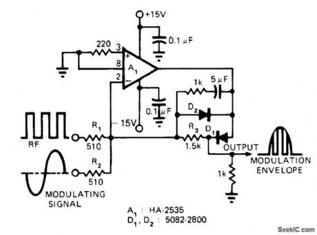
Developed to produce positive-going half-sine envelope modulated 100% by digital RF signal. Modulator uses loop gain of opamp to reduce diode drops very nearly to ideal zero level. D2, prevents opamp output terminal from swinging more negative than diode drop of 0.3V, which is not apparent at output. RF input amplitude must be sufficient to provide 100% modulation; this can be achieved by providing about 20% overdrive to give safety factor. Use hot-carrier diodes such as HP-2800 series.-D. L. Quick, Improve Amplitude Modulation of Fast Digital Signals, EDN Magazine, Sept. 20, 1975, p 68 and 70. (View)
View full Circuit Diagram | Comments | Reading(1695)
| Pages:1011/2234 At 2010011002100310041005100610071008100910101011101210131014101510161017101810191020Under 20 |
Circuit Categories
power supply circuit
Amplifier Circuit
Basic Circuit
LED and Light Circuit
Sensor Circuit
Signal Processing
Electrical Equipment Circuit
Control Circuit
Remote Control Circuit
A/D-D/A Converter Circuit
Audio Circuit
Measuring and Test Circuit
Communication Circuit
Computer-Related Circuit
555 Circuit
Automotive Circuit
Repairing Circuit