
Circuit Diagram
Index 1007
18_20000_Hz_SINE_SQUARE
Published:2009/7/7 1:42:00 Author:May
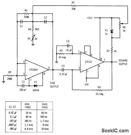
Circuit uses two opamps to obtain necessary positive feedback for sustaining osdllation. RC network of first stage acts astuned circuit, permhting operation only at frequency determined by values of R and C. Pot R3 provides tuning over significant frequency range. Pot R8 controls amplitude of sine output. Zener X1 stabilizes amplitude of square output. Sine signal is applied to LM111 acting as limiter to provide desired square wave. Table gives values of C1 and C2 for five different frequency ranges.-E. M .Noll, Linear IC Principles, Experiments, and Projects, Howard W.Sams, Indianapolis, IN, 1974, p 123-124. (View)
View full Circuit Diagram | Comments | Reading(588)
VARIABLE_SLOPE_COMPRESSOR_EXPANDER
Published:2009/7/7 1:40:00 Author:May
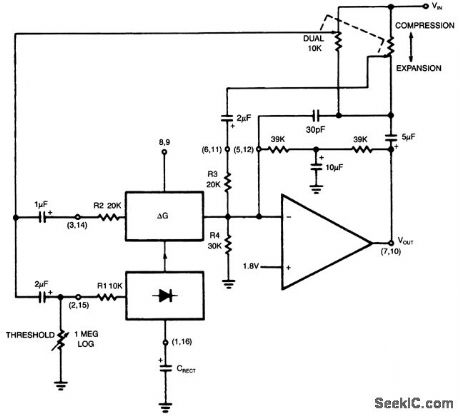
Compression and expansion ratios other than 2:1 can be achieved by the circuit shown. Rotation of the dual potentiometer causes the circuit hook-up to change from a basic compressor to a basic expander. In the center of rotation, the circuit is 1:1, has neither compression nor expansion. The (input) output transfer characteristic is thus continuously variable from 2:1 compression to 1:2 expansion. If a fixed compression or expansion ratio is desired, proper selection of fixed resistors can be used instead of the potentiometer. The optional threshold resistor will make the compression or expansion ratio deviate towards 1:1 at low levels. A wide variety of (input) output characteristics can be created with this circuit. (View)
View full Circuit Diagram | Comments | Reading(786)
Ring_counter_that_transfers_power_sequentially_to_a_series_of_n_loads
Published:2009/7/21 22:56:00 Author:Jessie
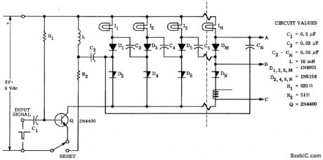
Ring counter that transfers power sequentially to a series of n loads (courtesy Motorola Semiconductor Products Inc.). (View)
View full Circuit Diagram | Comments | Reading(1052)
Direction_and_speed_control_for_shunt_wound_motors
Published:2009/7/21 22:54:00 Author:Jessie
This circuit is similar to that of Fig. 8-19, except that the shunt field is placed across the rectified supply and the motor armature is placed in the SCR bridge. Thus, the field current is always in the same direction, but the armature current is reversible, so the direction of rotation is reversible (as determined by which transformer, T1 or T2, is selected through the switch). Again, motor speed is set by R1. (View)
View full Circuit Diagram | Comments | Reading(0)
PLL_clock_for_an_ADC1100_BIN_dual_slope_A_D_convener
Published:2009/7/21 22:52:00 Author:Jessie
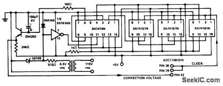
PLL clock for an ADC1100/BIN dual-slope A/D convener (courtesy Analog Devices, Inc.). (View)
View full Circuit Diagram | Comments | Reading(669)
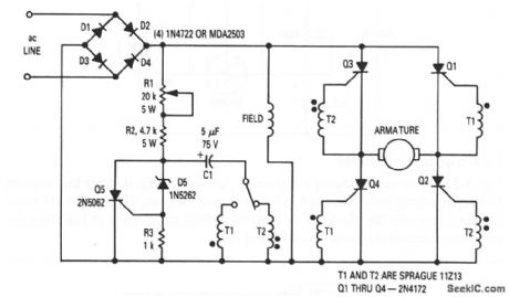
Direction_and_speed_control_for_series_wound_or_universal_motors
Published:2009/7/21 22:51:00 Author:Jessie
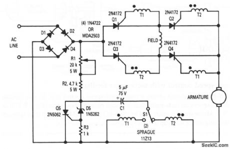
In this circuit, Q1 through Q4 are triggered in diagonal pairs. The pair to be turned on is controlled by S1, which selects either T1 or T2 to receive a pulse from Q5. Current in the motor field is reversed by selecting either Q2 and Q3, or Q1 and Q4, for conduction. Because motor armature current is always in the same direction, the field current reverses in relation to the armature current, which thus reverses the direction of motor rotation. The setting of R1 determines the conduction angle of either Q1 through Q4 or Q2/Q3, thus setting the average motor voltage and thereby the speed. (View)
View full Circuit Diagram | Comments | Reading(735)
DC_MOTOR_SPEED_CONTROLLER
Published:2009/7/7 1:39:00 Author:May
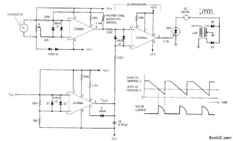
Tachometer driven by motor produces output voltage proportional to speed for application to CA3080A voltage comparator after rectification and filtering. Output of CA3080A is applied to upper CA3094A phase comparator that is receiving reference voltage from another CA3094A connected as ramp generator. Output of phase comparator triggers SCR in motor circuit. Amount of motor current is set by time du-ration of positive signal at pin 6, which in turn is determined by DC voltage applied to pin 3 of phase comparator by error detector. Circuit action serves to maintain constant motor speed at value determined by position of pot R. Input to ramp generator is pulsating DC voltage used to control rapid charging of C1 and slower discharging to form ramp.-E. M. Noll, Linear IC Principles, Experiments, and Projects, Howard W. Sams, Indianapolis, IN, 1974, p 321-323. (View)
View full Circuit Diagram | Comments | Reading(1758)
HI_FI_COMPRESSOR_WITH_PRE_EMPHASIS
Published:2009/7/7 1:38:00 Author:May
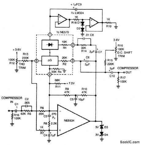
The compressor contains a high-frequency, pre-emphasis circuit (C2, R5, and C8, R14), which helps solve this problem. Matching de-emphasis on the expander is required. More complex designs could make the pre-emphasis variable. (View)
View full Circuit Diagram | Comments | Reading(1533)
LOW_VOLTAGE_COMPANDER
Published:2009/7/7 1:36:00 Author:May
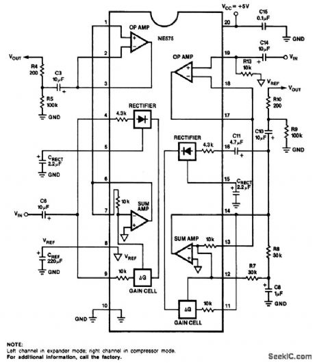
The NE575 is a dual-gain control circuit designed for low voltage applications. The NE575's channel 1 is an expander, while channel 2 can be configured either for expander, compressor,or automatic level controller (ALC) applications. (View)
View full Circuit Diagram | Comments | Reading(2188)
SINGLE_SUPPLY_MULTIVIBRATOR
Published:2009/7/7 1:27:00 Author:May

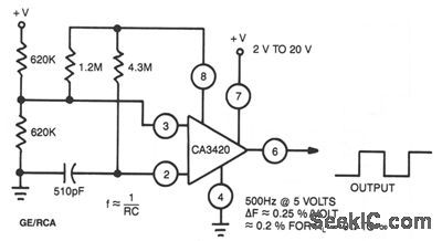
This multivibrator uses a CA3420 BiMOS op amp to provide improved frequency stability. The output frequency remains essentially independent of supply voltage. Because of the inherent buffering action of pin 6, frequency shift is approximately 0.2% when RL varies between zeroΩ to infinity. (View)
View full Circuit Diagram | Comments | Reading(640)
Long_time_delay_power_switch_for_porch_or_garage
Published:2009/7/21 22:49:00 Author:Jessie
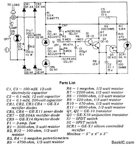
Long time delay power switch for porch or garage. The circuit can handle loads up to 500 watts (courtesy General Electric Company). (View)
View full Circuit Diagram | Comments | Reading(645)
Alternate_motor_speed_control_with_tachometer_feedback
Published:2009/7/21 22:48:00 Author:Jessie
This circuit is an alternate to that shown in Fig. 8-17, but with a lower parts count. The same magnet-coil tachometer shown in Figs. 8-17B and 8-17C can be used with the circuit of Fig. 8-18. Motor speed is controlled by the 100-kΩ pot. (View)
View full Circuit Diagram | Comments | Reading(1099)
FIXED_FREQUENCY_GENERATOR
Published:2009/7/7 1:25:00 Author:May
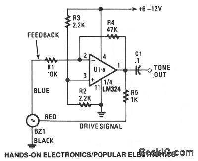
A single op amp, one fourth of an LM324 quad op amp, is configured as a standard inverting ampli-fter. At power up, a positive voltage is applied to the noninverting input of U1, via R3, forcing its output high. That high output travels along three paths. The first path is the tone output. Along the second path, by way of R5, that high is used as the drive signal for BZ1. In the third path, the high output of U1 is fed back, via R4, to the inverting input of U1. That forces U1's output to go low. And that low, when fed back to the inverting input of U1, causes the op amp output again to a high, and the cycle repeats itself. As configured, U1 provides a voltage gain of 4.7 (gain R4/R1).The outer ring of the piezo element is usually connected to the circuit ground. The large inner cir-cle serves as the driven area, and the small elon-gated section supplies the feedback signal. Resistor R5 sets BZ1's output-volume level. That level can be increased by decreasing R5 for example, to 470 Ω. To decrease the volume, increase R5 to about 2.2 KΩ, or so.Resistors R2 and R3 set the bias for op amp ,U1's positive input pin 3 to half of the supply-voltage level. That allows for a maximum voltage swing at U1's output. Although a quad op amp is specifted, almost any similar low cost single or dual op amp will work for U1a. (View)
View full Circuit Diagram | Comments | Reading(2172)
FILTER_TYPE_SSB_GENERATOR
Published:2009/7/21 22:47:00 Author:Jessie
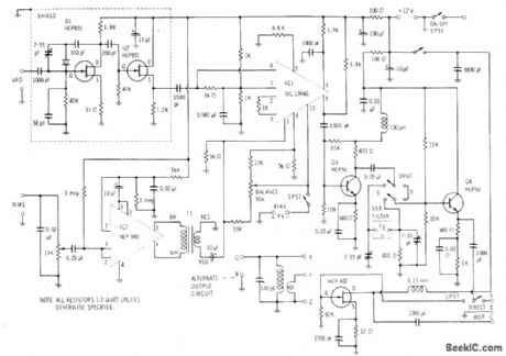
Carrier is generated by FET crystal oscillatorQ1 followed by buffer Q2. Modulating wave is applied to HEP 580 connected as two-stage audio amplifier feeding double-balanced modulator IC1 through transformer T1. Double-sideband signal from pin 6 of IC1 is applied to amplifier Q3-Q4 for straight-through amplification when double-sideband output is desired. For 9-MHz single-sideband operation, sideband filter is switched in between transistors.-E, M, Noll. Linear IC Principles, Experiments, and Projects. Howard W Sams, Indianapolis,IN,1974,p353-356. (View)
View full Circuit Diagram | Comments | Reading(1071)
Sequential_UJT_SCR_timer_circuit
Published:2009/7/21 22:45:00 Author:Jessie
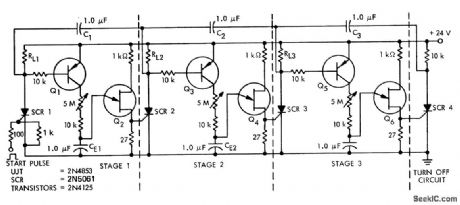
Sequential UJT-SCR timer circuit. This circuit is useful in washing machine circuits where different time cycles are required (courtesy Motorola Products Inc.). (View)
View full Circuit Diagram | Comments | Reading(1903)
VERSATILE_2φ_PULSE_GENERATOR
Published:2009/7/7 1:22:00 Author:May
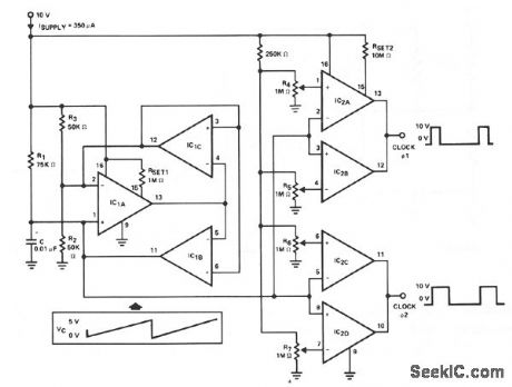
View full Circuit Diagram | Comments | Reading(809)
MONOSTABLE_MULTIVIBRATOR
Published:2009/7/7 1:21:00 Author:May
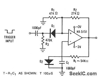
The circuit illustrates the usefulness of the HA-5151 as a battery-powered monostable. In this cir-cuit, the ratio is set to.632, which allows the time constant equation to be reduced to:T = RtCtD2 is used to force the output to a defined state by clamping the negative input at +0.6 V. Trigger-ing is set by C1, R3, and D2. An applied trigger pulls the positive input below the clamp voltage, +0.6 V, which causes the output to change state. This state is held because the negative input cannot follow the change because of Rt· Ct. This particu-lar circuit has an output pulse width set at approxi-mately 100 μs. Use of potentiometers for Rt and variable capacitors for Ct will allow for a wide variation in T. (View)
View full Circuit Diagram | Comments | Reading(2495)
PRECISION_AUDIO_WAVEFORM_GENERATOR
Published:2009/7/7 1:19:00 Author:May
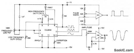
This circuit generates sinusoidal, square, and triangle waveforms simultaneously. Set the frequency to a particular value or vary it, as shown above. An op amp can be added for extra drive capability and simpli-fied amplitude adjustment. A simple comparator, slicing the triangle waveform, provides continuous duty cycle adjustment at a constant frequency. (View)
View full Circuit Diagram | Comments | Reading(1165)
POSITIVE_TRIGGERED_MONOSTABLE
Published:2009/7/7 1:18:00 Author:May
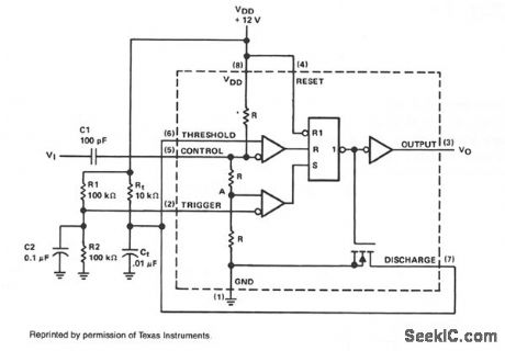
A positive-going trigger pulse can be used to start the timing cycle with the circuit shown. In this design, trigger input pin 2 is biased to 6 V (1/2 VDD) by divider R1 and R2. Control input pin 5 is biased to 8 V (2/3 VDD) by the internal divider circuit. With no trigger voltage applied, point A is at 4 V (1/3 VDD). To turn the timer on, the voltage at point A has to be greater than the 6 V present on pin 2. Positive 5-V trigger pulse VI applied to the control input pin 5 is ac coupled through capacitor C1, adding the trigger voltage to the 8 V already on pin 5; this results in 13 V with respect to ground. The output pulse width is determined by the values of Rt and Ct.When voltage at point A is increased to 6.5 V, which is greater than the 6 V on pin 2, the timer cycle is initialized. The output of timer pin 3 increases, tuming off discharge transistor pin 7 and allowing Ct to charge through resistor Rt. When capacitor Ct charges to the upper threshold voltage of 8 V( 2/3 VDD), the flip-flop is reset and output pin 3 decreases. Capacitor Ct then discharges through the discharge transistor. The timer is not triggered again until another trigger pulse is applied to control input pin 5. (View)
View full Circuit Diagram | Comments | Reading(687)
CLIPPER
Published:2009/7/21 22:44:00 Author:Jessie
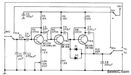
Combined speech amplifier and logarithmic clipper for use with SSB transmitters reduces speech bandwidth to about 500-3000 Hz, with very little distortion. Power can be obtained from separate battery or from transmitter itself.-Circuits, 73 Magazine, March 1977, p 152. (View)
View full Circuit Diagram | Comments | Reading(1925)
| Pages:1007/2234 At 2010011002100310041005100610071008100910101011101210131014101510161017101810191020Under 20 |
Circuit Categories
power supply circuit
Amplifier Circuit
Basic Circuit
LED and Light Circuit
Sensor Circuit
Signal Processing
Electrical Equipment Circuit
Control Circuit
Remote Control Circuit
A/D-D/A Converter Circuit
Audio Circuit
Measuring and Test Circuit
Communication Circuit
Computer-Related Circuit
555 Circuit
Automotive Circuit
Repairing Circuit