
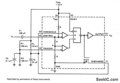
Circuit Diagram
Index 1008
LOW_FREQUENCY_FM_GENERATORS
Published:2009/7/7 1:14:00 Author:May
Here are two FM generators for low frequency, less than 0.5 MHz center frequency, applications. Each uses a 566 function generator as a modulation generator and a second 566 as the carrier generator. Capacitor C1 selects the modulation frequency adjustment range and C1 selects the center frequency. Capacitor C2 is a coupling capacitor which only needs to be large enough to avoid distorting the modulating waveform. If a frequency sweep in only one direction is required, the 566 ramp generators given in this section can be used to drive the center generator. (View)
View full Circuit Diagram | Comments | Reading(1128)
HARMONICS_GENERATOR
Published:2009/7/7 1:12:00 Author:May
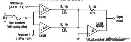
Two comparators and a summing amplifier that generate differential harmonic spectra comprise a sim-ple frequency multiplier. The resulting circuit can extract harmonics from a sine, triangle, sawtooth, or any other sloping-sided waveform. With a sloped-input waveform, a comparator produces an output pulse width that's proportional to the input amplitude plus a reference voltage. Changing the reference can vary the pulse width from 0 to 100%. As the pulse width changes, the harmonic spectrum changes, but two comparators combined in the adder eliminate harmonics, depending on the duty cycle. For example, a 50% pulse will lack all the even-num-bered harmonics. Similarly, a 25% duty-cycle pulse will be missing multiples of the fourth harmonic and deliver the second, sixth, and tenth harmonics. Accordingly, the circuit generates multiples of the input frequency that might not have existed in the input waveform. Adjusting the references can create virtually any harmonic. Because comparators A1 and A2 supply differential inputs to the added A3, the adder cancels out equal harmonics. Therefore, both A1 and A2 should have identical ac characteristics, and A3 should have good common-mode rejection and a high slew rate. In particular, R1, R2, and R3 should match within 0.1%. Of course, the accuracy of the circuit depends heavily on the amplitude stability of the input. (View)
View full Circuit Diagram | Comments | Reading(1074)
POWER_TRANSISTOR_TEST_GATE
Published:2009/7/21 22:32:00 Author:Jessie
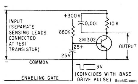
Rectangular pulse opens saturated amplifier; gate output is then ct series of pulses whose amplitude is equal to voltage across power transistor under lest when full load current is drawn.-D. H. Breslow, Measuring Parameters by Power Transistor Pulse Techniques, Electronics, 34:1, p 120-122. (View)
View full Circuit Diagram | Comments | Reading(760)
LOW_COST_FSK_GENERATOR
Published:2009/7/7 1:07:00 Author:May
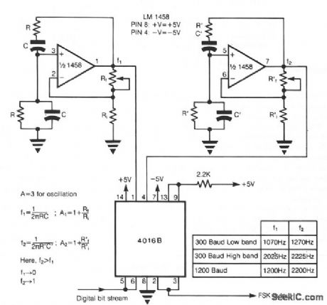
In FSK, two discrete frequencies are used to represent the binary digits0 and 1. The heart of the circuit consists of two Wien-bridge oscillators built using a dual op amp LM 1458, for the two frequencies. The two frequencies are enabled corresponding to digital data using two switches in SCL 4016. The control lines of these switches are logically inverted with respect to each other using one of the switches in SCL 4016 as an inverter, so as to enable only one oscillator output at a time. The digital bit stream is used to control the analog switches as shown. Since the switching frequency limit of SCL 4016 is 40 MHz, high-data rates can be easily accommodated. This method comes in handy when expensive FSK generator chips are not readily available; also, the components used in this circuit are easily available off the shelf and are quite cheap. (View)
View full Circuit Diagram | Comments | Reading(1153)
XOR_GATE_COMPLEMENTARY_SIGNALS_GENERATOR
Published:2009/7/7 1:05:00 Author:May
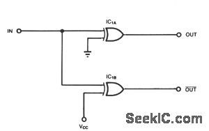
Some applications, such as driving three-state buffers for data multiplexers or for biphase clocks in high-speed systems, require complementary signals having a small-time skew and nearly simultaneous transitions. Here, XOR gates function as both inverting and noninverting gates. For CMOS systems, practically any type of XOR gate will work. However, the advanced-CMOS logic (ACL) families have the greatest drive capability, the shortest gate delays, and the tightest manufacturing tolerances. For TTL systems, compatible CMOS types such as the ACT or S/AS86 families are preferable. Do not use low-power TTL versions (LS or ALS), because they have large propagation delay differences when one XOR gate is inverting and the other is noninverting. (View)
View full Circuit Diagram | Comments | Reading(755)
LOW_COST_TRANSISTOR_TESTER
Published:2009/7/21 22:31:00 Author:Jessie
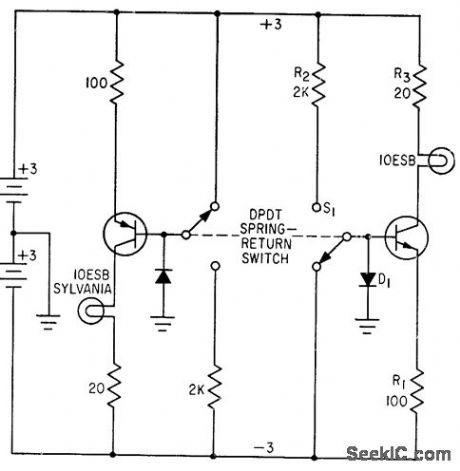
Indicates, in one simple operation, whether transistor has had catastrophic failure and, if not, whether it can provide minimum data (gain) of 20 at 30 ma. Test circuit is inverter with emitter degeneration resistor R1 providing control of collector current during warm up of indicator lamp.-E. H. Sommerfield, Simple Transistor Tester Uses Lamp for Indicator, Electronics, 34:36, p 80. (View)
View full Circuit Diagram | Comments | Reading(764)
NONINTEGER_PROGRAMMABLE_PULSE_DIVIDER
Published:2009/7/7 1:04:00 Author:May
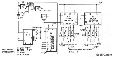
The purpose of D-type flip-flop IC2 is to synchronize the input signal with the clock pulse. When the clock pulse changes from low to high and the input is high, IC2 output is high. Subsequently, IC3 resets to zero and starts counting up. Until the counter counts to ten, the counter is inhibited. Thus, the number of pulses of the output of IC3 is ten times input pulse. The designed frequency of the clock pulse must be ten times higher than the maximum frequency of the input. IC4 and IC5 are cascaded to form a two decade programmable down counter. Since the number of pulses appearing at the input of the down counter is ten times the input to the divider, the effective range of the divisor for this divider is 0.1 to 9.9. (View)
View full Circuit Diagram | Comments | Reading(1896)
PROGRAMMABLE_TRIANGLE__SQUARE_WAVE_GENERATOR
Published:2009/7/7 1:02:00 Author:May
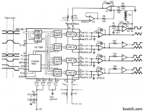
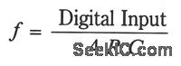
The programmable multiple output generator provides the control signals for data converter ATE. Major performance criteria are simple, interfaces to a number of microprocessor systems, low power con-sumption, stable output timing relationships combined with a minimum of board space. For schematic sim-plicity only, one output circuit is shown in full.The monolithic HS7584 provides four current output DAC's with four quadrant multiplication, individ-ual reference input and a feedback resistor. The digitally controlled integrator's frequency is determined by:C is the value of C1 to C4 andfi is the resistance of the DAC. With the four DACS on a single chip, the resistance matching is good, which results in stable timing relationships of the generator outputs. The out-put of the comparator A2 determines whether the constant current source provided by A3 and A4 is posi-tive or negative. (View)
View full Circuit Diagram | Comments | Reading(1061)
Overvoltage_protection_for_telephone_equipment
Published:2009/7/21 22:31:00 Author:Jessie
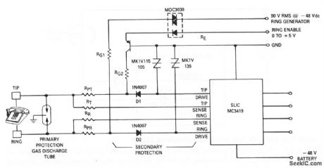
This circuit shows two SIDACs that are connected to protect the telephone Subscriber Loop Interface Circuit (SLIC) and associated electronics from voltage surges. This is in addition to the primary protection provided by the gas-discharge tube across the tip and ring lines. If a high positive-voltage transient appears on the lines, D1 (with a peak-inverse voltage of 1000 V) blocks the pulse, and the corresponding SIDAC conducts the surge to ground. Conversely, D2 and the related SIDAC protect the SLIC from negative transients. The SIDACs do not conduct when normal signals are present. (View)
View full Circuit Diagram | Comments | Reading(1968)
CLASSIC_OP_AMP_ASTABLE_MULTIVIBRATOR
Published:2009/7/7 1:00:00 Author:May
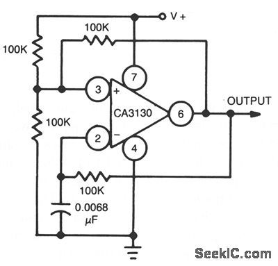
Uses CA3130 BiMOS op amp that operates at a frequency of 1 kHz. With rail-to-rail output swing, frequency is independent of supply voltage, device, and temperature. 0nly the temperature coefficient of RT and CT enters into circuit stability. (View)
View full Circuit Diagram | Comments | Reading(1471)
Motor_speed_control_with_tachometer_feedback
Published:2009/7/21 22:44:00 Author:Jessie
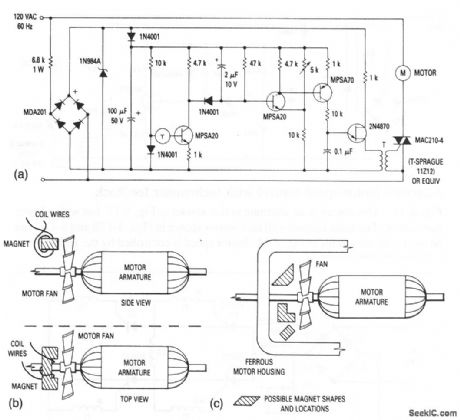
This circuit shows a triac motor-speed control that derives feedback from a magnet-coil tachometer that is placed near the motor fan (Figs. 8-17B and 8-17C). Motor speed is controlled by the 5-kΩ pot. The MAC210-4 triac is capable of handling motor loads up to 10 A. (View)
View full Circuit Diagram | Comments | Reading(3199)
SIDEBAND_SELECTOR_MOSFET
Published:2009/7/21 22:44:00 Author:Jessie
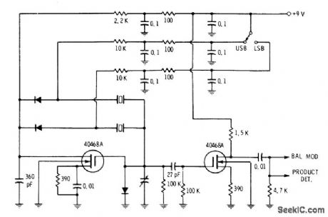
circuit uses diode switching of crystals in carrier oscillator to select either upper or lower sideband. Second transistor serves as common-source isolating amplifier for driving modulator. Switch applies +9V to anode of diode that closes feedback circuit for crystal to be activated. Developed for use in SSB transceiver; if operating in 9-MHz range, crystals can be 8.9985 MHz and 9.0015 MHz.-E. M. Noll, FET Principles, Experiments, and Projects, Howard W. Sams, Indianapolis, IN, 2nd Ed., 1975, p 191-192. (View)
View full Circuit Diagram | Comments | Reading(1008)
Time_delay_circuit_using_a_UJT_and_two_SCRs
Published:2009/7/21 22:41:00 Author:Jessie
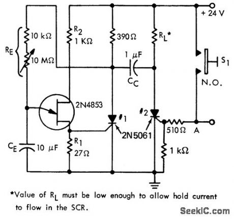
Time delay circuit using a UJT and two SCRs. Time delay is determined by setting of 10M pot from less than a second to approximately 2.5 minutes (courtesy Motorola Semiconductor Products Inc.). (View)
View full Circuit Diagram | Comments | Reading(959)
Motor_speed_control_with_load_current_feedbac
Published:2009/7/21 22:41:00 Author:Jessie
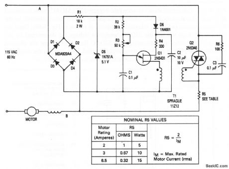
This circuit shows a triac motor-speed control that derives feedback from the load current and does not require separate connections to the motor field and armature windings. Thus, this circuit can be conveniently built into an appliance or used as a separate control, When the triac conducts, in response to signals from Q1 through T1, the normal line voltage (less the drop across the triac and R5) is applied to the motor. By delaying the firing of the triac until a later portion of the cycle, the voltage applied to the motor is reduced (or controlled) and speed is reduced proportionally. The use of feedback maintains torque at reduced speeds. The angle at which Q1 fires is proportional to motor current (and the setting of R3) because Q1 is controlled by the voltage across points A and B. As the motor is loaded and draws more current, the firing angle of Q1 is advanced, causing a proportional increase in the voltage applied to the motor, and a consequent increase in the available torque. (View)
View full Circuit Diagram | Comments | Reading(5458)
Time_delay_circuit_using_a_UJT
Published:2009/7/21 22:40:00 Author:Jessie
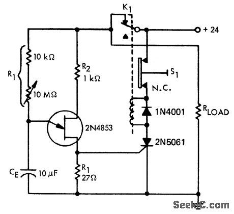
Time delay circuit using a UJT. Maximum time delay is set by the 10M pot. Time delay can be set from less than a second to approximately 2.5 minutes (courtesy Motorola Semiconductor Products Inc.). (View)
View full Circuit Diagram | Comments | Reading(1401)
FUNCTION_GENERATOR
Published:2009/7/7 0:59:00 Author:May
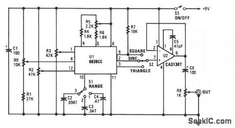
This circuit can output sine, square, and triangular signals of from 15 Hz to 25kHz in three ranges. The circuit is built around an 8038 function generator that produces the triangular- and square-wave out-puts directly from an oscillator. The triangular output is then processed to develop the sine waze. While that method doesn't provide a sufficiently low level of distortion to let you make distortion measurements on audio gear, the degree of purity is high enough for frequency-response tests and a lot of other audio analysis. Three switched capacitors, C2 to C4, set the circuits frequency range via switch S1. Variable resistor R9 and resistor R1 provide the voltage for controlling the charge and discharge rates of the timing capacitor selected. Resistors R4 to R6 control the charge and discharge currents. Resistor R5 can be adjusted to provide a 1.1 mark/space ratio. (View)
View full Circuit Diagram | Comments | Reading(0)
LOGARITHMIC_LIMITER
Published:2009/7/21 22:38:00 Author:Jessie
Speech processor with logarithmic limiting makes noticeable improvement in speech readability of SSB transmitter. Adjustable-gain preamp U1 sets input level for soft limiting amplifier U2 in which nonlinear resistance characteristics of CR1 and CR2 supply increasingly heavier negative feedback as U2 output amplitude increases, thus providing logarithmic response. Low-pass active filter using U3 attenuates any frequencies above 2.8 kHz that may be generated in clipping process.-F. C. Getz, Audio-Frequency Speech Processor, Ham Radio, Aug. 1977, p 48-51. (View)
View full Circuit Diagram | Comments | Reading(1399)
FOUR_OUTPUT_WAVEFORM_GENERATOR
Published:2009/7/7 0:57:00 Author:May
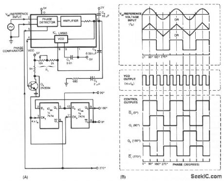
Many applications require control signals that have phase shifts with reference to an input signal. Circuit acceptsa sine, square, or triangular wave as an input reference signal and produces square-wave out-puts with 0°, 90°, 180°,and 270° phase shifts with respect to the input. Figure 38-3B shows the input and output waveforms. The circuit contains two ICs: an LM565 phase-locked loop and a 7474 dual-D posi-tive edge-triggered flip-flop. R1 and C1 set the free-running frequency of the LM565's VCO. You should adjust RI so that the frequency is approximately four times that of the input reference signal. The LM565 responds to input signals greater than 10 mV pk-pk; 3 V pk-pk is the,hipb maximum allowable input level. Q1 matches the LM565's output to the flip-flops' inputs. The flip-flops' outputs provide the TTL-compati-ble square-wave signals with 0°, 90°, 180°, and 270° phase shift with reference to the input signal. (View)
View full Circuit Diagram | Comments | Reading(2128)
24_hour_clock_without_the_1_hertz_reference_circuitry
Published:2009/7/21 22:37:00 Author:Jessie
24-hour clock without the 1-hertz reference circuitry. It provides seconds, minutes and hours (courtesy Motorola Semiconductor Products Inc.). (View)
View full Circuit Diagram | Comments | Reading(1424)
LINEAR_TRIANGLE_WAVE_TIMER
Published:2009/7/7 0:53:00 Author:May
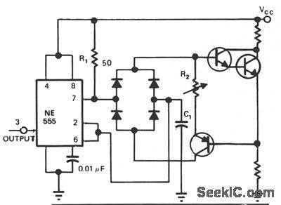
Using one current source for the charge and discharge path in this circuit ensures identical rise and fall times at the capacitor terminal. A Darlington pair ensures identical biasing of the IC during the charge and discharge cycles. The period of the triangle wave is: T ≈ 0.46VC1/R2. VCC must be at least 8 V to maintain linearity. At the output at pin 3 of the IC timer, a 50% duty-cycle square wave, frequency tunable by R2 alone, appears. (View)
View full Circuit Diagram | Comments | Reading(855)
| Pages:1008/2234 At 2010011002100310041005100610071008100910101011101210131014101510161017101810191020Under 20 |
Circuit Categories
power supply circuit
Amplifier Circuit
Basic Circuit
LED and Light Circuit
Sensor Circuit
Signal Processing
Electrical Equipment Circuit
Control Circuit
Remote Control Circuit
A/D-D/A Converter Circuit
Audio Circuit
Measuring and Test Circuit
Communication Circuit
Computer-Related Circuit
555 Circuit
Automotive Circuit
Repairing Circuit