
Circuit Diagram
Index 1017
CHARGE_COMPENSATED_SAMPLE_AND_HOLD
Published:2009/7/6 21:15:00 Author:May

Circuit NotesLess than±5 pC charge transfer(less than 5 mV sample-to-hold offset when CL=1000 pF). (View)
View full Circuit Diagram | Comments | Reading(719)
SYNCHRONIZING__TWO__MICROPROCES_SORS
Published:2009/7/6 21:15:00 Author:May
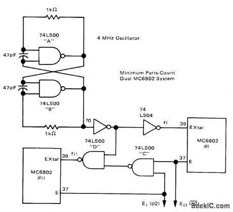
4-MHz oscillator using 74LS00 quad two-input NAND gates serves in place of crystal source of individual MC6802 microprocessors to ensure synchronizing so one microprocessor operates during half-cycle when other microprocessor is disabled Arrangement gives computing power of two MPUs with system cost of one data bus. No time is sacrificed since half-cycle used would normally be dead time on bus.-J. Farrell, “Synchronizing Two Motorola MC6802s on One Bus,” Motorola, Phoenix, AZ,1978, AN-783. (View)
View full Circuit Diagram | Comments | Reading(859)
INFINITE_SAMPLE_AND_HOLD_AMPLIFIER
Published:2009/7/6 21:12:00 Author:May
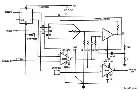
Circuit NotesDuring normal hold mode, the replicated analog voltage is buffered straight through the S/H amplifier to the output. Upon issuance of a SAMPLE signal, the SiH amplifier is placed in the hold mode, holding the voltage until the new analog voltage is valid. The same SAMPLE signal triggers an update to the input sample-and-hold amplifier. The most current analog voltage is captured and held for conversion. The previously deter-mined voltage is held stable at the output during the conversion cycle while the SAR/D-to-A converter continuously adjusts to replicate the new input voltage. At the end of the conversion, the output sample-and-hold amplifier is once again placed in the track mode. The new analog voltage is then regenerated. (View)
View full Circuit Diagram | Comments | Reading(787)
1700_MHz_VCO_CIRCUIT
Published:2009/7/22 3:37:00 Author:Jessie
This VCO circuit is for 1700 MHz and uses a ceramic coaxial resonator (View)
View full Circuit Diagram | Comments | Reading(2095)
05_Hz_TO_1_MHz_SINE_SQUARE_TRIANGLE_
Published:2009/7/6 21:10:00 Author:May
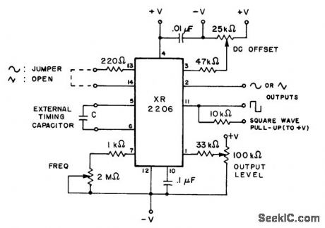
Uses Exar XR-2206 IC function generator in simple circuit that operates from dual supply ranging from ±6 V to ±12 V. Withl-μF capacitor for C, 2-megohm frequency control covers range of 0.5-1000 Hz. Range is 5-10,000 Hz with 0.1 μF, 50 Hz to 100 kHz with 0.01 μF, and 500 Hz to 1 MHz with 0.001 μF. Designed for experiments with active filters.-H. M. Berlin, Design of Active Filters, with Experiments, Howard W.Sams, Indianapolis, IN, 1977, p 9-10, (View)
View full Circuit Diagram | Comments | Reading(8059)
TWO_TONE_ALARM
Published:2009/7/6 21:07:00 Author:May
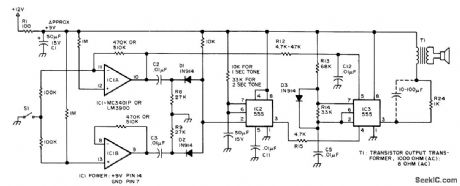
Provides audible backup for visual display in microprocessor-controlled system that requires human intervention under certain conditions, to alert operator who may be watching machinery rather than display. When input line goes high, device emits 1-s beep that means stop. When input goes low, 1-s lower-frequency boop sounds to indicate go. S1 represents signal derived from single-bit computer output. Audio bursts are generated by 555 timers, IC2 is wired as mono MVBR to determine tone duration, set by C4 and R11.Negative-going pulse on pin 2 triggers mono on. ff microprocessor circuit creates pulse rather than level change, input should go to pin 2. Tone frequency is set by C5, R13, and R14 of IC3. Trigger uses IC1A as inverting opamp and IC1B as noninverting opamp. Trigger outputs are differentiated to give negative-going spike for each input level change. Spikes are ORed by Dl and D2 for trigger input of IC2. Different tones are achieved by using IC1A to change input voltage to pin 5 of tone generator IC3. 0p-tional electrolytic capacitor across R24 will in-crease volume.-C. F. Douds, Audible Interrupts for Humans, BYTE, Feb. 1977, p 54 and 58. (View)
View full Circuit Diagram | Comments | Reading(935)
TRANSMISSION_LINE_RESONATOR_VCO_CIRCUIT
Published:2009/7/22 3:36:00 Author:Jessie
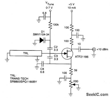
The figure shows a typical VCO circuit using a transmission-line resonator and varactor tuning. This circuit is for 855 to 890 MHz. (View)
View full Circuit Diagram | Comments | Reading(1240)
800_W_soft_start_light_dimmer
Published:2009/7/22 3:35:00 Author:Jessie
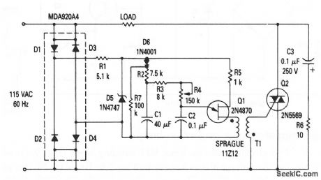
This circuit shows the basic UJT building block (Fig. 9-1), which is used in a light dimmer with soft-start operation that applies current to the light slowly enough to eliminate high surges (high inrush current). These current surges, found in most cold-filament light dimmers, shorten lamp life. With this circuit, the lamp is heated slowly by a gradually increasing voltage so that inrush current is kept to a minimum. R4 controls the charging rate of C2 and provides the means to control or dim the lamp. (View)
View full Circuit Diagram | Comments | Reading(0)
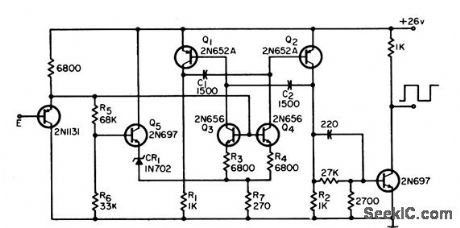
WIDE_FREQUENCY_TTL_CLOCK
Published:2009/7/6 21:06:00 Author:May
This free-running TTL square-wave oscillator has a variable frequency output over a 20:1 range or better through use of four of the six inverters in an SN7404 chip and the additional components shown.Frequency of oscillation is determined by the capacitor and the settings of potentiometers R2 and R4; the first pot controls width T1 and the second controls width T2 of the square-wave output. These adjustments are not completely independent. (View)
View full Circuit Diagram | Comments | Reading(947)
SINGLE_OP_AMP_CLOCK
Published:2009/7/6 21:05:00 Author:May
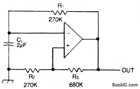
Capacitor C1 is charged through timing resistor R1 when the clock output is high. When C1 reaches the upper threshold voltage, the output signal decreases, and then C1 discharges through R1 until its voltage reaches the lower threshold point. When this happens, the output increases again and the cycle repeats itself. Using the parts values shown results in a frequency of 1 Hz. The output frequency can be adjusted by trimming the value of R1 slightly. (View)
View full Circuit Diagram | Comments | Reading(791)
AF_SQUELCH_AMPLIFIER
Published:2009/7/22 1:18:00 Author:Jessie
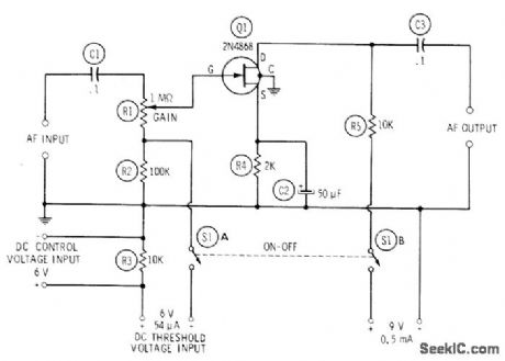
Holds audio channel of receiver silent until receiver input signal reaches predetermined amplitude. DC control voltage can be derived from IF amplifier by rectification or from second detector of receiver. FET is biased to cutoff by DC gate voltage applied to threshold terminals. DC control voltage bucks this bias and activates amplifier when-ever it exceeds predetermined threshold in range of 0-6 V. If receiver gives opposite polarity for DC voltages, use P-channel FET such as 2N2608, reverse C2, and change R4 and R5 as required.-R. P. Turner, FET Circuits, Howard W. Sams, Indianapolis, IN, 1977, 2nd Ed., p 73-74. (View)
View full Circuit Diagram | Comments | Reading(875)
VOLTAGE_CONTROLLED_NONLINEAR
Published:2009/7/6 21:05:00 Author:May

Circuit produces function E0 = Xy/12, where X is input voltage in range of +10 mV to +10 V and Y is analog programming voltage in range of -0.4 V to -10 V. Uses Optical Electronics 2534 temperature-compensated log feedback elements, +5 V reference, two high-frequency opamps, and one low-frequency opamp. 2534 produces log conversion of input signal. 5898 multiplier serves to vary scale factor of log signal. With offsets used as shown, +10 V input will always produce +10 V output regardless of Y input. To set up, adjust R4 until output does not change with Y for +10 V input, then adiust R7 for +10 V output with +10 V input.- Voltage- Controlled Non-Linear Function Generator, Optical Electronics, Tucson, AZ, Application Tip 10263. (View)
View full Circuit Diagram | Comments | Reading(701)
R_C_COUPLED_BASE_MODULATION
Published:2009/7/22 1:17:00 Author:Jessie
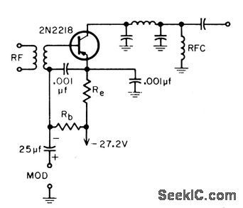
Modulation signal is injected by using two resistors, volues of which are determined by available r-f drive power; higher power is needed for larger resistance values. Excellent linearization of waveform is obtained with Re from 10 to 30 ohms. Rb should be in range from 100 to 2,000 ohms, with 470 as good com promise value. Modulation of 100% is easily achieved for CB transmitter.-B. Rheinfelder, Modulation Techniques for Transistorized A-M Transmitters, EEE, 11:7, p 54-57. (View)
View full Circuit Diagram | Comments | Reading(798)
OSCILLATOR_CLOCK_GENERATOR
Published:2009/7/6 21:04:00 Author:May
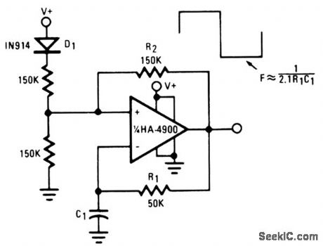
This self-starting fixed-frequency oscillator circuit gives excellent frequency stability. R1 and C1 comprise the frequency-determining network, while R2 provides the regenerative feedback.Diode D1 enhances the stability by compensating for the difference between VOH and VSUPPLY. In applications where a precision clock generator up to 100 kHz is required, such as in automatic test equipment, C1 might be replaced by a crystal. (View)
View full Circuit Diagram | Comments | Reading(1580)
SAMPLE_AND_HOLD_CIRCUIT_II
Published:2009/7/6 21:03:00 Author:May

Circuit Notes
This circuit rapidly charges capacitor Csto to a voltage equal to an input signal. The input signal is then electrically disconnected from the capacitor with the charge still remaining on Csto Since Csto is in the negative feedback loop of the operational amplifier, the output voltage of the amplifier is equal to the voltage across the capacitor.Ideally, the voltage across Csto should remain constant causing the output of the amplifier to remain constant as well. However, the voltage across Csto will decay at a rate proportional to the current being injected or taken out of the current summing node of the amplifier. This current can come from four sources: leakage resistance ofCsto, leakage current due to the solid state switch SW2, currents due to high resistance paths on the circuit fixture, and most important, bias current of the operational amplifier. If the ICH8500A operational amplifier is employed, this bias current is almost non-existent (less than 0.01pA). Note that the voltages on the source, drain and gate of switch SW2 are zero or near zero when the circuit is in the hold mode. Careful construction will eliminate stray resistance paths and capacitor resistance can be eliminated if a quality capacitor is selected. The net result is a low drift sample and hold circuit.The circuit can double as an integrator. In this application the input voltage is applied to the integrator input terminal. The time constant of the circuit is the product of R1 and Csto. (View)
View full Circuit Diagram | Comments | Reading(1782)
LINEAR_F_M_MODULATOR
Published:2009/7/22 1:17:00 Author:Jessie
Adding emitter-followers to useable mvbr makes output frequency linear function (within 0.01%) of input voltage for 50% modulation above and below center frequency.-G. Richwell, Linear FM Modulator, EEE, 12:10, p 59-60. (View)
View full Circuit Diagram | Comments | Reading(663)
TEMPERATURE_CONTROL
Published:2009/7/6 21:01:00 Author:May
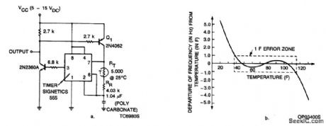
A couple of transistors and a thermistor in the charging network of the 555 type timer enable this device to sense temperature and produce a corresponding frequency output. The circuit is accurate to within ±1 Hz over a 78°F temperature range. (View)
View full Circuit Diagram | Comments | Reading(0)
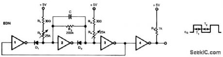
LOGGING_EXACT_TIME
Published:2009/7/6 21:01:00 Author:May
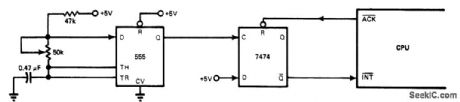
Used in microcomputer applications requiring recording of exact time of each event by data-logging printer,Uses555 timer and 7474 D flip-flop to produce interrupt request every 16.67 ms. Requires use of software routine that acknowledges interrupt, increments counter in known location to serve as time-of-day clock, and resumes interrupted program,Article diagrams software routine required. –Real-Time Software keeps Program Segments on Schedule, EDN Magazine. Novm,20.1976,p277-283. (View)
View full Circuit Diagram | Comments | Reading(618)
SIGLE_CONTROL_FOR_1000000;1_FREQUENCY_RANGE
Published:2009/7/6 21:00:00 Author:May
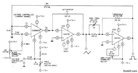
Uses two RCA CA313 opamps and CA3080A operational transconductance amplifier to generate square and triangle outputs that can be swept over range of o.1 Hz to 100 kHz with single 100K pot R1. Altemate voltage-control input is available for remote adiustment of sweep frequency. IC1 is operated as voltage-controlled current source whose output current is applied directly to integrating capacitor C1 in feedback loop of integrator IC2. R2 adiusts symmetry of triangle output. IC3 is used as controlled switch to set excursion limits of triangle output when square wave is desired.- Linear Integrated Circuits and MOS/FET's, RCA Solid State Division, Somerville, NJ, 1977, p 236-244 (View)
View full Circuit Diagram | Comments | Reading(664)
DUO_DIODE_HALF_WAVE_SWITCH_MODULA_TOR
Published:2009/7/22 1:14:00 Author:Jessie
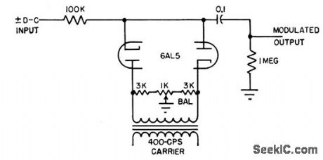
Tube serves in place of chopper. Carrier voltage turns diodes on and off, transferring d-c input signal to output when diodes are not conducting. With 10-v rms carrier voltage, output is linear up to 2 v for inputs up to 5 v d-c.-L. S. Klivans, Modulators for Automatic Control Systems, Electronics, 31:1, p 82-84. (View)
View full Circuit Diagram | Comments | Reading(871)
| Pages:1017/2234 At 2010011002100310041005100610071008100910101011101210131014101510161017101810191020Under 20 |
Circuit Categories
power supply circuit
Amplifier Circuit
Basic Circuit
LED and Light Circuit
Sensor Circuit
Signal Processing
Electrical Equipment Circuit
Control Circuit
Remote Control Circuit
A/D-D/A Converter Circuit
Audio Circuit
Measuring and Test Circuit
Communication Circuit
Computer-Related Circuit
555 Circuit
Automotive Circuit
Repairing Circuit