
Circuit Diagram
Index 1002
TEMPERATURE_SENSING_TD_OSCILLATOR
Published:2009/7/21 21:46:00 Author:Jessie
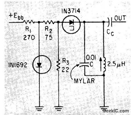
Mylar capacitor with known and reproducible temperature characteristics makes oscillator frequency vary with temperature, Diode bias regulator circuit is used.-E. Gottlieb and J. Giorgis, Tunnel Diodes-Using Them as Sinusoidal Generators, Electronics, 36:24, p 36-42. (View)
View full Circuit Diagram | Comments | Reading(754)
LOW_HYSTERESIS_D_C_LEVEL_DETECTOR
Published:2009/7/21 21:46:00 Author:Jessie
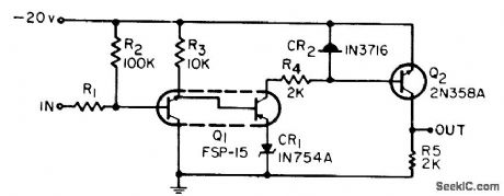
Serves as temperature control when thermistor or other temperature-sensing resistive device is connected to input. Dual complementary transistor Q1 is high-stability d-c amplifier, with zener diode CR1 providing threshold level. With sharp-breaking charatcteristic for zener, hysteresis con be less than 10 mv between turn-on end turn-off. -P. C. Murray, Accurate DC-Level Detector, EEE, 13:12, p 65. (View)
View full Circuit Diagram | Comments | Reading(721)
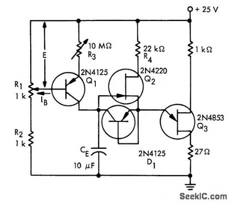
PROPORTIONING_TEMPERATURE_CONTROL
Published:2009/7/21 21:44:00 Author:Jessie
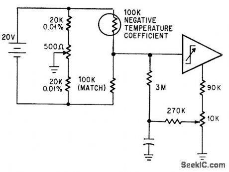
Operational trigger trips when temperature goes beyond 0.001℃ of desired value. Bridge power supply is floating.-P. Lefferts, Operational Trigger For Precise Control, Electronics, 37:28, p 50-55. (View)
View full Circuit Diagram | Comments | Reading(687)
COPROCESSOR_SOCKET_DEBUGGER
Published:2009/7/7 3:17:00 Author:May
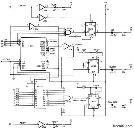
The IBM PC debugger plugs into the PC's math-coprocessor socket.The 8288 bus controller, IC1, regenerates control signals from the processor's status signals, S0, S1, and S2. Reset LED D1 lights if reset is active and holding the processor. Clock status LED D3 indicates that the processor is receiving a toggling clock signal. The address-decode logic detects when the processor is doing a jump-on-reset to the PC's BIOS ROM's power-on; self-test then detects a fatal error and halts the processor.
(View)
View full Circuit Diagram | Comments | Reading(1224)
Long_duration_time_delay_circuit
Published:2009/7/21 21:43:00 Author:Jessie
Long duration time delay circuit. Time delays of up to 10 hours are possible with this circuit (courtesy Motorola Semiconductor Products Inc.). (View)
View full Circuit Diagram | Comments | Reading(747)
DIGITAL_THERMOCOUPLE_THERMOMETER
Published:2009/7/7 3:16:00 Author:May
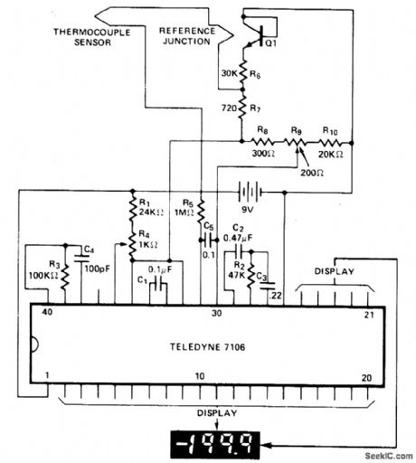
This digital thermocouple thermometer uses one active component and 15 passive components. With this circuit, both type J and type K thermocouples may be used. The type J will measure over the temperature range of 10 to 530℃ with a conformity of ±2℃. The type K will measure over a temperature range of 0℃ to 1000℃ with a conformity of ±3℃. (View)
View full Circuit Diagram | Comments | Reading(3373)
HIGH_ACCURACY_CONTROL
Published:2009/7/21 21:43:00 Author:Jessie
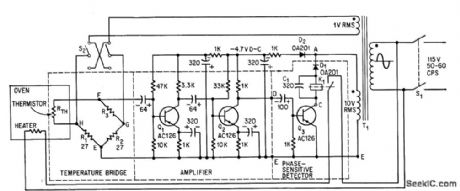
Holds temperature constant to within 0.1℃for any value between -25 and 200℃. For controlling refrigerated unit instead of oven, switch S2 is placed in its other position and output relay is then used to energize solenoid valve that controls fiow of refrigerant.-G. H. P. Kohnke, Electronic Thermostat Controls Temperature to Within 0.1℃,Electronics, 39:1,P 100-102. (View)
View full Circuit Diagram | Comments | Reading(675)
OPAMP_SPEED_CONTROL
Published:2009/7/7 3:16:00 Author:May
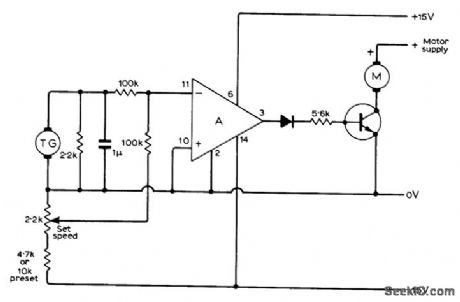
Provides fine speed control of DC motor by using 0.25-W 6-V motor as tachogenerator giving about 4 V at 13,000 rpm. Opamp (RCA 3047A or equivalent) pro-vides switching action for transistor in series with controlled motor, up to within a few volts of supply voltage. Choose transistor to meet motor current requirement.-N. G. Boreham, D.C. Motor Controller, Wireless World, Aug.1971, p 386. (View)
View full Circuit Diagram | Comments | Reading(1611)
DIGITAL_THEREMIN
Published:2009/7/7 3:15:00 Author:May
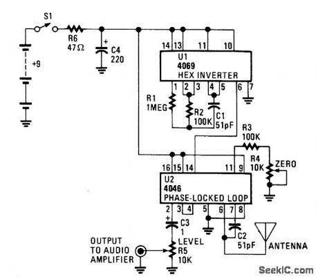
The CD4069 or 74C04 hex inverter-is used as a fixed-frequency oscillator centered around 100 kHz. U2 contains the variable frequency oscillator and balanced modulator.The CD4046 is a phase-locked loop and R3, R4, and C2 determine the center frequency of the on-chip oscillator. The antenna forms a parallel capacitance with C2, which allows the frequency to be shifted several kilohertz by bringing a hand near the antenna. R4, the ZERO control, allows the variable oscillator to be set to the same frequency as the fixed oscillator. When the difference frequency is below 15 Hz, it is below the lower frequency limit of the ear. By setting both oscillators to the same frequency, the Theremin remains silent until the performer brings his or her hand near the antenna. The oscillators are mixed by an exclusive OR gate inside the 4046. That gate acts as a digital balanced modulator, which produces the sum and difference frequencies. The output of the gate is then ac coupled by C3 to LEVEL control R5 and an output jack for connection to an audio amplifier or stereo receiver.
(View)
View full Circuit Diagram | Comments | Reading(3373)
SPARE_FLIP_FLOP_INVERTER
Published:2009/7/7 3:14:00 Author:May
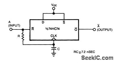
The circuit uses one-half of a dual D flip-flop as an inverter. When the input decreases, the flip-flop resets, and its Q output increases. When the input increases, the reset line is released and Q gets clocked low. The rc delay between applying the input signal to the flip-flop's reset input and its clock input enables clocking the flip-flop on the input's positive edge. A 74HC74 dual D flip-flop, for example, requires a minimum recovery time of 5 ns after releasing the reset input before strobing its clock input. Therefore, speccing rc at greater than 7.5 ns provides adequate margin. The slight slowing of the clock edge presents no problem, because the clock input's maximum allowable rise time is a much longer 500 ns. To prevent skewing of the output's symmetry, limit the maximum input frequency to less than 10 MHz.
(View)
View full Circuit Diagram | Comments | Reading(813)
WATER_LEVEL_CONTROL
Published:2009/7/7 3:14:00 Author:May
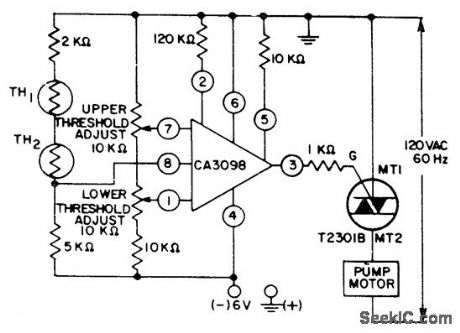
Two thermistors operating in self-heating mode are mounted on sides of water tank. Thermistors change resistance when water level rises so liquid rather than air conducts heat away. Threshold adjustment pots are set so RCA CA3098 programmable Schmitt trigger turns on pump motor when water level rises above thermistor mounted near upper edge of tank, to remove water from tank and prevent overflow. Motor stays on to pump water out of tank until water level drops below location of lower thermistor inside tank.- Linear Integrated Circuit and MOS/ FET's, RCA Solid State Division, Somerville, NJ, 1977, p 218-221. (View)
View full Circuit Diagram | Comments | Reading(2688)
ELECTRONIC_THEREMIN
Published:2009/7/7 3:13:00 Author:May

This circuit has the CMOS IC doing double-duty performance,The first two mvertersoperate as a digital audio oscillator;the third operates as a low-gain linear audio amplifier,As the intensity of the light falling on photoresistor LDR1 mcreases the oscillator's frequency Increases;similarly,the illumination falling on photoresistor LDR2 determinesthe volume level from the loudspeaker:The more illumination the more volume.If you flop and wave your hands between the two photocells and a light source,a special kind of electronic muslc will be produced. (View)
View full Circuit Diagram | Comments | Reading(969)
Four_stage_ring_counter_using_SUS_devices
Published:2009/7/21 22:17:00 Author:Jessie
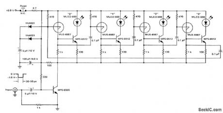
Four-stage ring counter using SUS devices (courtesy Motorola Semiconductor Products Inc.). (View)
View full Circuit Diagram | Comments | Reading(1083)
RS_232C_LED_CIRCUIT
Published:2009/7/7 3:13:00 Author:May
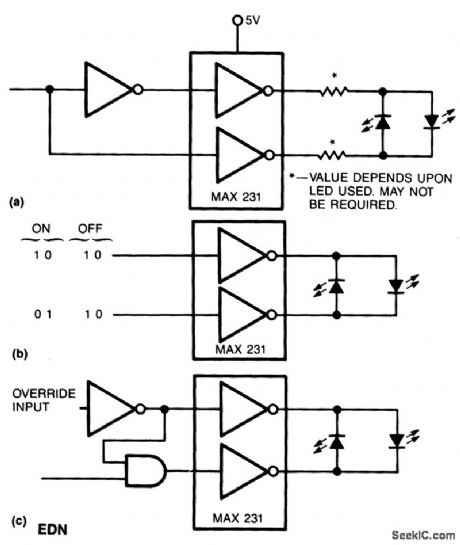
Use a pair of Maxim's 5V-powered MAX231 RS-232C transmitters as drivers to obtain a 2-color LED. The transmitters require only a singleended, 5-V input to generate ±10 V internally.Their outputs are short-circuit-proof and can supply as much as 10 mA-enough to drive most LEDs.Depending on which LED you select, their currentlimiting feature might also eliminate the need for external series resistors. Using the simple circuits, you can implement a variety of functions.
(View)
View full Circuit Diagram | Comments | Reading(878)
SPIKE_CLIPPER
Published:2009/7/21 22:16:00 Author:Jessie
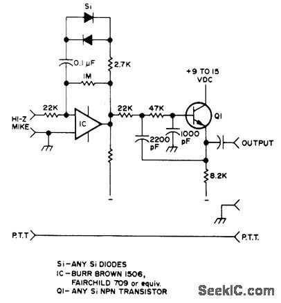
Improves efficiency of low-power SSB amateur transmitter by removing from voice waveform the spikes that cause over modulation or give low average modulation level. When used as in-line microphone amplifier, circuit gives up to 20-dB equivalent gain at receiving location.-H. E. Weber, Increase Your SSB Efficiency, 73 Magazine, Dee. 1973, p 71. (View)
View full Circuit Diagram | Comments | Reading(949)
DIODE_TESTER_1
Published:2009/7/21 22:16:00 Author:Jessie
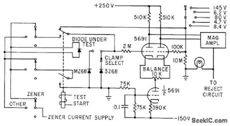

Three-triode constant-current difference amplifier triggers magnetic amplifier that drives reject mechanism of automatic zener voltage tester for diodes.-E. V. Marrott and V. S. Zucco, High-Speed Automatic Diode Tester, Electronics, 34:2, p 93-95. (View)
View full Circuit Diagram | Comments | Reading(716)
Zero_crossing_switch_for_sensitive_gate_SCRs
Published:2009/7/21 22:15:00 Author:Jessie
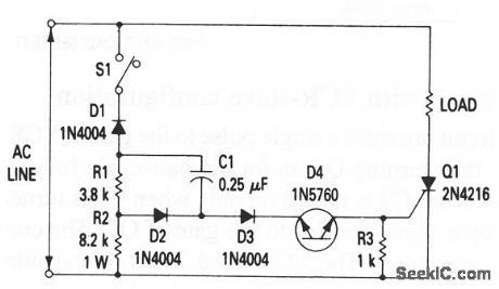
This circuit is primarily for sensitive-gate SCRs, such as the 2N4216, and loads of 1.5 A or less. (View)
View full Circuit Diagram | Comments | Reading(712)
CRYSTAL_BFO
Published:2009/7/21 22:14:00 Author:Jessie
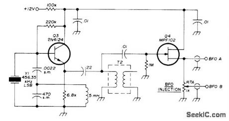
Bipolar crystal oscillator is coupled to FET source-follower by miniature 455-kHz IF transformer T2. RF output is adjusted with R7A so BFO injection voltage can be set for maximum carrier suppression. BFO is 456.35 kHz for lower sideband operation or 453.75 kHz for upper sideband in SSB transceiver.-W. J. Weiser, Integrated Circuit SSB Transceiver for 80 Meters, Ham Radio, April 1976, p 48-52. (View)
View full Circuit Diagram | Comments | Reading(3976)
PARAMP_TEST_SET
Published:2009/7/21 22:14:00 Author:Jessie
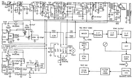
Supplies c-w signal that can be injected into parametric amplifier under test, and indicates relative power output of paramp on meter. Test set also has 30-Mc output for feeding automatic noise-figure meter.-C. F. Brett, Parometric Amplifier for Space Probe Tracking, Electronics, 34:4, p 41-45.
(View)
View full Circuit Diagram | Comments | Reading(1255)
INDUCTION_MOTOR_SPEED
Published:2009/7/7 3:10:00 Author:May

Uses variable-frequency UJT oscillator at upper left to toggle MC664 RS flip-flop which in turn clocks MC663 JK flip-flops. Quadrature-phased JK outputs are combined with fixed-width pulses in MC672 to provide zero-voltage steps of drive signals for phase A and phase B. Outputs of RS flip-flops are differentiated and positive-going transitions amplified by pair of 2N3904 transistors, with pulse width of about 500μs. NAND-gate outputs are then translated by small-signal amplifiers to levels suitable for driving final transistors having complementary NPN/PNP pairs .Circuit will provide speed range of 300 to 1700 rpm for permanent-split capacitor motor.-T. Mazur , Variable Speed Control System for Induction Motors, Motorola, Phoenix, AZ, 1974, AN-7A, p 6. (View)
View full Circuit Diagram | Comments | Reading(1393)
| Pages:1002/2234 At 2010011002100310041005100610071008100910101011101210131014101510161017101810191020Under 20 |
Circuit Categories
power supply circuit
Amplifier Circuit
Basic Circuit
LED and Light Circuit
Sensor Circuit
Signal Processing
Electrical Equipment Circuit
Control Circuit
Remote Control Circuit
A/D-D/A Converter Circuit
Audio Circuit
Measuring and Test Circuit
Communication Circuit
Computer-Related Circuit
555 Circuit
Automotive Circuit
Repairing Circuit