
Circuit Diagram
Index 1269
5_V_CROWBAR
Published:2009/6/28 22:39:00 Author:May
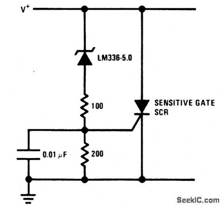
View full Circuit Diagram | Comments | Reading(1)
_5_V_from___5_V_at_mediurn_power_lowo_noise_
Published:2009/7/25 4:10:00 Author:Jessie
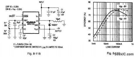
Figure 8-118 shows a MAX735 PWM regulator connected to provide -5 V at medium power. Figure 8-119 shows the efficiency curves. The input voltage range is 4 V to 6.2 V, with a quiescent current of 1.6 mA (VIN = 5 V), a maximum load current of 200 mA (VIN = 5 V), and a shutdown current of 10 μA. MAXIM BATTERY MANAGEMENT CIRCUIT COLLECTION, 1994, P. 58. (View)
View full Circuit Diagram | Comments | Reading(662)
The relay low-power maintenance
Published:2011/7/21 1:59:00 Author:Seven | Keyword: low-power, maintenance circuit
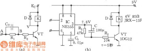
The pulling in current of the relay is high that its releasing current, when the relay pulls in, the relay will working while keeping the state. See as the figure, the circuit can make the relay working in a low current after it pulls in, so the power consumption is reduced. When the 3-pin of 555 is turned into the high LEV from the low, as the voltage on C can't mutate, so the input current that VT acquires is (VA-0.7V)/R2. After that, C is charged by R2 and eb Knot, VB is falling down, when C is full, VB=VA-Vc. (View)
View full Circuit Diagram | Comments | Reading(644)
FAST_ACTING_POWER_SUPPLY_PROTECTION
Published:2009/6/28 22:38:00 Author:May
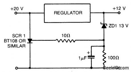
When using a regulated power supply to reduce a supply voltage, there is always the danger that component failure in the power supply might lead to a severe overvoltage condition across the load. To cope with overvoltage situations, the circuit is designed to protect the load underovervoltage conditions. Component values given are for a 20 V supply with regulated output at 12 V. The zener diode can be changed according to whatever voltage is to be the maximum. If the voltage at the regulator output rises to 13 V or above, the zener diode breaks down and triggers the thyristor which shorts out the supply line and blows the main fuse. (View)
View full Circuit Diagram | Comments | Reading(881)
74 Series digital circuit of 74273,74LS273 eight D flip-flop (with clear side)
Published:2011/8/1 1:42:00 Author:Lucas | Keyword: 74 Series , digital circuit , eight D flip-flop , (with clear side
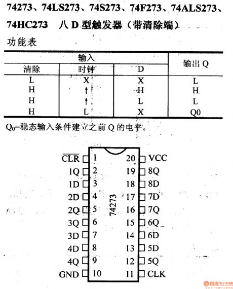
Q0 = the output level before establishing the steady-state input conditions.
(View)
View full Circuit Diagram | Comments | Reading(2899)
IC_function_generator_connected_for_sine_output_without_external_adjustment
Published:2009/7/25 3:58:00 Author:Jessie
This circuit is similar to that of Fig. 5-31, except that the circuit is connected for sine outputs (S1 closed). R1 at pin 7 provides frequency tuning. Output swing is greater than V+/2, and typical distortion (THD) is less than 2.5%.If lower sine distortion is desired, use Fig. 5-33. If a triangle output is desired, open S1. The circuit can be used with a split supply by replacing all ground connections with V-, and connect R3 to ground (View)
View full Circuit Diagram | Comments | Reading(892)
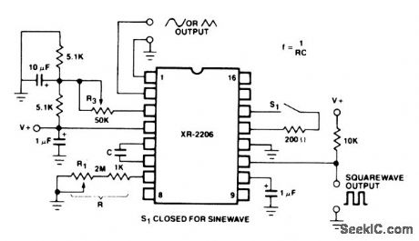
Basic_IC_function_generator
Published:2009/7/25 3:57:00 Author:Jessie
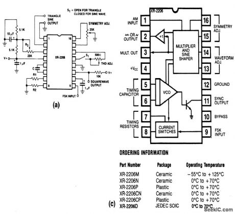
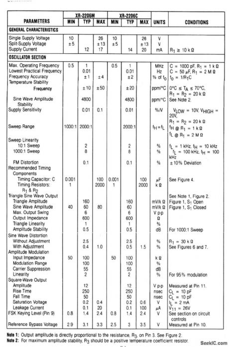
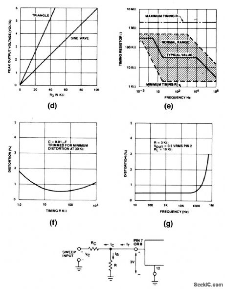
This circuit uses an XR-2206 to provide sine,square,triangle,ramp and pulse output waveforms, which can be both amplitude and frequency modulated Electrical characteristics and functional circuits of the XR-2206 are shown in Figs 5-31B and C, respectively, The operating frequency is set by capacitor C between puts 5 and 6.The THD ADJ pot between pins 13 and 14 adjusts the waveform.R3 sets the amplitude(Fig.5-31D)The SYMMETRY ADJ pot between pins 15 and 16 is a fine waveform adjustment.Open S1 for triangle, close S1 for sine.The square output is at pin 11 .See Conditions in Fig. 5-31B (View)
View full Circuit Diagram | Comments | Reading(4094)
OVERVOLTAGE_PROTECTION_FOR_LOGIC
Published:2009/6/28 22:37:00 Author:May
Zener diode ZD1 senses the supply, and the should the supply rise above 6 V, Q1 will turn on. In turn, Q2 conducts clamping the rail. Subsequent events depend on the source supply. It will either shut down, go into current limit or blow its supply fuse. None of these will damage TTL chips. The rating of Q2 depends on the source supply, and whether it will be required to operate continuously in the event of failure. Its current rating has to be in excess of the source supply. (View)
View full Circuit Diagram | Comments | Reading(1033)
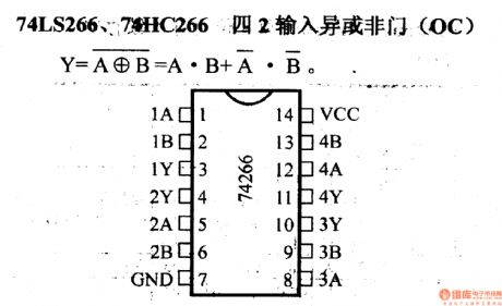
74 Series digital circuit of 74LS266,74HC266 four 2 input XNOR(OC)
Published:2011/8/1 4:25:00 Author:Lucas | Keyword: 74 Series , digital circuit , four 2 input, XNOR, OC
View full Circuit Diagram | Comments | Reading(2005)
IC_waveform_generator_for_high_level_pulse_and_square_wave_output
Published:2009/7/25 3:54:00 Author:Jessie
This circuit is similar to that of Fig. 5-28, except the circuit provides high-level pulse (S2 closed) or square (S2 open) outputs. Duty cycle of the pulse is controlled by RD. The amplitude and polarity of either pulse or square output is controlled by Rq. See Conditions in Fig. 5-28B. (View)
View full Circuit Diagram | Comments | Reading(787)
OIL_PRESSURE_DISPLAY
Published:2009/6/28 22:37:00 Author:May
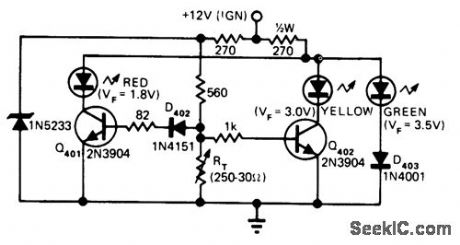
Bed, yellow, and green LEDs give positive indication of oil pressure levelon electronic gage console developed for motorcycle. Transducer converts oil pres-sure to variable resistance RT, which in turn varies bias on transistors. LEDs have different forward voltages at which they light, so proper selection of bias resistors ensures that only one LED is on at a time to give desired indication of oil pressure.-J. D. Wiley, Instrument Console Features Digital Displays and Built-In Combo Lock, EDN Magazine, Aug, 5, 1975, p 38-43. (View)
View full Circuit Diagram | Comments | Reading(749)
IC_waveform_generator_with_split_supply_and_AM_FM_modulation_output
Published:2009/7/25 3:52:00 Author:Jessie

This circuit is similar to that of Fig. 5-28, except that the circuit is operated from a split-supply and provides for AM modulation at pin 3, or FM modulation at pin 13. See Conditions in Fig. 5-28B. (View)
View full Circuit Diagram | Comments | Reading(994)
74 Series digital circuit of 74265 four complementary output circuit
Published:2011/8/1 1:40:00 Author:Lucas | Keyword: 74 Series , digital circuit, four complementary output
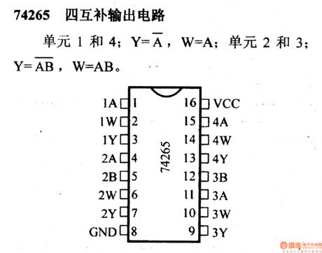
Units 1 and 4; Y=A,W=A; units 2 and 3; Y=AB, E=AB.
(View)
View full Circuit Diagram | Comments | Reading(808)
BUZZER_FOR_IDIOT_LIGHT
Published:2009/6/28 22:36:00 Author:May
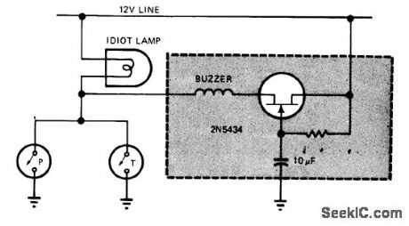
Provides audible supplement to engine-monitoring indicator lamps that are often difficuh to see in daylight. Uses 2N5434 JFET to provide delay of about 7 s each time ignition switch isturned on,to allow for peaceful starting of car and normal buildup of oil pressure when lamp is monitoring oilpressure and engine-temperature sensors. Entire circuit can be mounted inside plastic housing of unused or disconnected dashboard warning buzzer in late-model car.-P. Glower, Audio Assist Gives Idiot Lights the Buzz. EDN Magazine, June 20, 1976, p 126. (View)
View full Circuit Diagram | Comments | Reading(742)
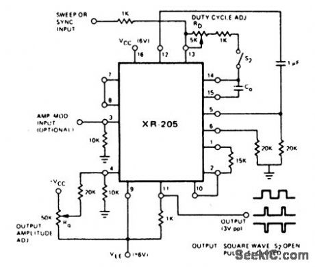
Basic_IC_waveform_generator
Published:2009/7/25 3:52:00 Author:Jessie
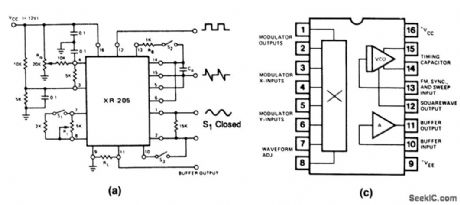
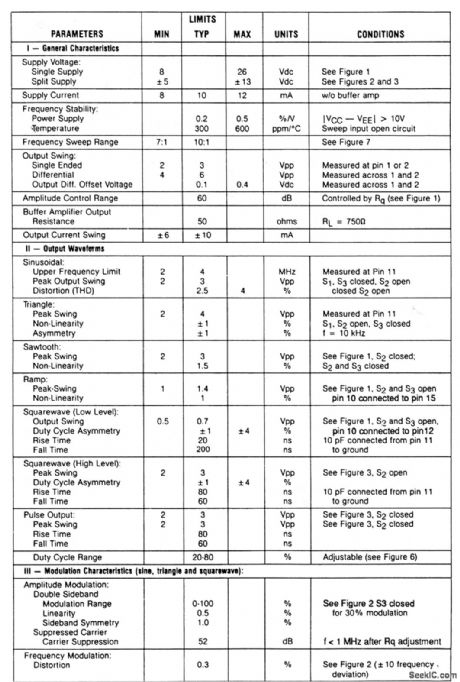
This circuit uses an XR-205 to provide sine, square, triangle, ramp and sawtooth output waveforms, which can be both amplitude and frequency modulated. Electrical characteristics and functional circuits of the XR-205 are shown in Figs. 5-28B and 5-28C, respectively. The operating frequency is set by capacitor Co between pins 14 and 15. With the sweep input open-circuited, the output frequency: f0 (in Hz) =400/C0 (inμF). The Rj pot between pins 7 and 8 adjusts the waveform. The Rq, pot at pin 4 sets the amplitude. For a triangle output at pins 1 and 2 (or pin 11 if the internal buffer is used), both S1 and S2 are open and S3 is closed. For a sine output, open S2, close S1 and S3, adjust Rj for minimum harmonic distortion, and Rq for a maximum output of about ± 3 Vpp. For a sawtooth output, open S1, close S2/S3. For a ramp output at pin 11 (of about 1.4 Vpp) open S3. The ramp duty cycle is controlled by RB across pins 13-14 or 13-15 (duty cycle decreases as RB is decreased). See Conditions in Fig. 5-28B. (View)
View full Circuit Diagram | Comments | Reading(2474)
74 Series digital circuit of 74LS261 2 × 4-bit parallel binary multiplier
Published:2011/8/1 20:04:00 Author:Lucas | Keyword: 74 Series , digital circuit , 2 × 4-bit parallel , binary multiplier
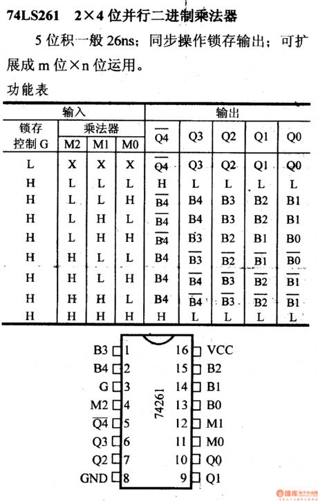
5-bit is general 26ns; synchronization latch output; it can be extended to m-bit × n-bit application.
(View)
View full Circuit Diagram | Comments | Reading(1975)
OVERVOLTAGE_PROTECTION_WITH_AUTOMATIC_RESET
Published:2009/6/28 22:35:00 Author:May
View full Circuit Diagram | Comments | Reading(924)
Low_distortion_oscillator
Published:2009/7/25 3:47:00 Author:Jessie
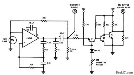
This circuit provides in-phase sine and TTL outputs at 1 kHz, with 1/4-W output drive. The symmetry-adjust pot is trimmed so that the edges of the TTL output precisely line up with the zero crossing of the sine output. (View)
View full Circuit Diagram | Comments | Reading(0)
74 Series digital circuit of 74LS257A,74F257 4-bit 2-to-1 data selector(tristate,in-phase)
Published:2011/7/25 4:27:00 Author:Lucas | Keyword: 74 Series, digital circuit , 4-bit , 2-to-1 data selector, tristate, in-phase
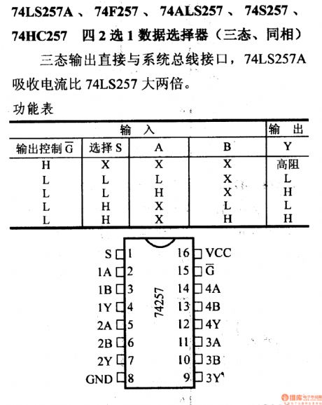
Three-state output is directly connected to the bus interface of the system, and 74LS257SA absorption current is 2 times larger than the 74LS257.
(View)
View full Circuit Diagram | Comments | Reading(1169)
144_MHz_FOR_VSWR_BRlDGE
Published:2009/6/28 22:32:00 Author:May
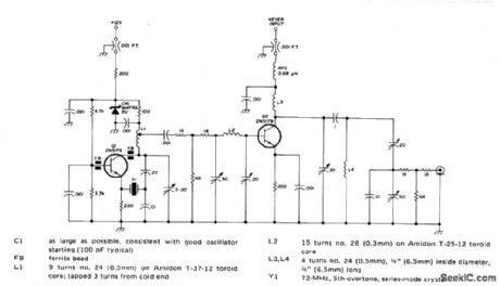
Modulated signal source provides 10-mW CW output and 5mW modulated output at modulation frequency of 1000 Hz. Spurious and harmonic outputs are 40 dB below desired output. 72-MHzcrystal oscillator is followed by doubler stage. attenuation between generator and load. Use Oscillator runs continuously while doubler is regulated power supply or batteries.-J. flei-keyed whh simple ON/OFF square-wave keying, Freedom from load variations is obtained with double-tuned output filter providing up to 6-dB attenuation between generator and load, Use regulated power supply or batteries.-J.Reisert, Matching Techniques for VHF/UHF Antennas, Ham Radio, July 1976, p 50-56. (View)
View full Circuit Diagram | Comments | Reading(843)
| Pages:1269/2234 At 2012611262126312641265126612671268126912701271127212731274127512761277127812791280Under 20 |
Circuit Categories
power supply circuit
Amplifier Circuit
Basic Circuit
LED and Light Circuit
Sensor Circuit
Signal Processing
Electrical Equipment Circuit
Control Circuit
Remote Control Circuit
A/D-D/A Converter Circuit
Audio Circuit
Measuring and Test Circuit
Communication Circuit
Computer-Related Circuit
555 Circuit
Automotive Circuit
Repairing Circuit